Download
1 / 29
300 likes | 454 Vues
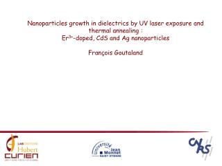
Nanoparticles growth in dielectrics by UV laser exposure and thermal annealing : Er 3+ -doped, CdS and Ag nanoparticles François Goutaland. Outline of the talk. Few words about me Facilities in the lab Project : different kinds of nanoparticles i n various dielectrics

E N D
Nanoparticles growth in dielectrics by UV laser exposure and thermal annealing : Er3+-doped, CdS and Ag nanoparticles François Goutaland
Outline of the talk • Few words about me • Facilities in the lab • Project : different kinds of nanoparticles in various dielectrics • aims of the project • results up to now • perspectives
Few words about me • research assistant (teaching/research) : University of Saint-Etienne, Hubert Curien Laboratory, UMR CNRS 5516 • PhD (1998) on defects in silica and germanosilicate optical fibers • One year post-doc (1999-2000) in the Optoelectronics Research Centre, University of Southampton (UK) : Er3+ -doped glass and glass-ceramics (telecom applications)
Few words about me • Research Activities • experimental physics • Rare Earth (Er3+) doped glass and glass ceramics • defects in silca-based glasses: UV-induced, thermal annealing… • more recently, nanoparticles (LaF3, SC, silver) in silica-based glasses • glass manufacturing : melt-quenching technique
Facilities associated with the « nanoparticles project » • spectroscopy • spectrometers : UV(above 200 nm), visible and IR (up to 1.5 µm) Raman, emission spectra (photon counting mode or CCD) • spectrophometer : from 200 to 900 nm • Absorption spectra • lasers • visible : Argon, He-Ne, He-Cd, 532 nm (spectroscopy) • IR: Ti:Sa cw (750-980 nm) or fs (800 nm) (either spectroscopy or laser processing) • UV : 244 nm cw (double frequency argon laser), 248 nm KrF (laser processing), 355 nm
Facilities associated with the « nanoparticles project » • detection • photomultiplier (visible and IR soon), photon counting, lock-in-amplifier • glass manufacturing • Pt crucible, furnaces: 1800°C and 1100°C (post-annealing), brass mould, optical polishing and cutting… • silica-based glasses (Ge-doped or not), Na2CO3, LaF3, CaCO3… • Er3+-doped glasses • Differential Thermal Analysis • RT 1200 °C • microscopy • high resolution MEB should soon be in used
Project : Nanoparticles in dielectrics • people involved • several research assitants and professors and two PhD students • Aims of the project • localisation of NP in dielectrics • NP growth : laser irradiation and/or thermal annealing • physical mechanisms of NP growth • different kinds of NP: Er3+-doped LaF3, Semiconductors , metallic (silver) • optical properties • theoritical aspect • various hosts: either bulk glasses or sol-gels
Project : Nanoparticles in dielectrics • history in the laboratory • Project started in 2005 • up to now: succesful with Er3+ in LaF3 nanoparticles (silicate and germanate glasses), silver and sulfur • home-made glasses in case of Er3+ and silver • Schott glasses for semiconductor particles
Hole ( few mm) UV laser beam cw, 244nm Project : Nanoparticles in dielectrics • Experimental techniques for NP growth • simultaneous heating and laser exposure experimental setup
Project : Nanoparticles in dielectrics • Experimental techniques for NP growth • UV density controlled by the focal lens • accurate spot size measurements • several laser irradiation wavelentghs available : KrF( 248 nm), YAG (355 nm), YAG (532 nm), Argon (244 nm) • femtosecond @ 800 nm • heating temperature up to 1100°C • separate steps (heating and UV exposure)
Project : Nanoparticles in dielectrics • Glass and NP characterization • DTA : determination of the crystallisation (TC) and annealing (TA) temperatures DTA curve
Project : Nanoparticles in dielectrics • Glass and NP characterization • Raman spectra : NP size • absorption and fluorescence spectra : optical properties Raman spectrum of CdS-doped glass
Project : Nanoparticles in dielectrics • Glass manufacturing • Pt crucible • furnace up to 1800 °C • starting with mixing powder (SiO2, GeO2, CaCo3, Na2CO3, …) • melt-quenching into a brass mould • furnace up to 1100°C for post annealing treatments • cutting and optical polishing
Project : Nanoparticles in dielectrics • Er3+ ions in different dielectrics • germanate glasses : collaboration with M. Mortier from Laboratoire de Chimie Appliquée de l'Etat solide, UMR CNRS 7574, Ecole Nationale Supérieure de Chimie de Paris • tellurite glasses : collaboration with Centre d’Etudes et de Recherches Lasers et Applications (CERLA), Université des Sciences et Technologies de Lille • germanosilicate glasses : home-made glasses
Project : Nanoparticles in dielectrics • Er3+ in germanate and tellurite glasses DTA measurements
Project : Nanoparticles in dielectrics • Er3+ in germanate glasses Emission spectroscopy PbF2 nanocrystals
Project : Nanoparticles in dielectrics • Er3+ in tellurite glasses Emission spectroscopy No crystal structure yet
Project : Nanoparticles in dielectrics • Er3+ in germanosilicate glasses
Project : Nanoparticles in dielectrics • Conclusions about Er3+ in glasses • strong reduction of the emission bandwidth : characteristic of a more symmetric environment (crystal like shape) • higher radiative intensities : reduction of the phonon energy thus of the non-radiative losses • raman spectrum : hard task because of the large fluorescence bands • Long irradiation times : difficult to change the Er3+ environment
Project : Nanoparticles in dielectrics • CdS nanoparticles (Schott glasses) • CdSxSe(1-x) • Low Frequency Raman spectroscopy • UV + heating • Nanoparticles
Project : Nanoparticles in dielectrics • CdS nanoparticles (Schott glasses) • Raman spectroscopy
Project : Nanoparticles in dielectrics • CdS nanoparticles (Schott glasses) • absorption spectroscopy • redshift of the absorption cut-off with the NP size
Project : Nanoparticles in dielectrics • Conclusions CdS nanoparticles • NP growth succesful • long irradiation times required : slow UV-induced process • raman spectrum : useful to demonstrate the early stages of crystallisation • absorption spectroscopy : redshift corresponding to NP growth
Project : Nanoparticles in dielectrics • Silver nanoparticles • home-made silica-based glasses • silver concentration up to 0.2% (wt) • absoption spectroscopy : nanoparticles plasamon resonance band at around 410 nm + NP size • raman spectroscopy : NP size
Project : Nanoparticles in dielectrics • Silver nanoparticles • NP growth succesful • absorption due to plasmon resonance @410 nm
Project : Nanoparticles in dielectrics • Silver nanoparticles • experimental conditions change the NP size • thermal annealing only: bigger NP
Project : Nanoparticles in dielectrics • Silver nanoparticles • UV influence solely : formation of Ag atoms due to electron trap • conversion fo Ag atoms into NP due to high temperature
Project : Nanoparticles in dielectrics • Silver nanoparticles : perspectives • very small particles compared to the usual case • NP growth very sensitive to annealing temperature • two stepes process : • Ag+ Ag (UV exposure) • nAg Agn(thermal annealing) • similar work is just starting with sol-gel matrix
Project : Nanoparticles in dielectrics • general perspectives • promising results up to now • much shorter UV irradiation times in case of Er3+ and CdS • by changing the glass matrix or the NP composition • by switching from glass to sol-gel • periodic structures in case fo silver NP • detailed investigations of the NP formation processes