Motivation and Design Issues
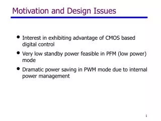
Motivation and Design Issues. Interest in exhibiting advantage of CMOS based digital control Very low standby power feasible in PFM (low power) mode Dramatic power saving in PWM mode due to internal power management. SVDD. PVIN. comparator. digital controller. SW. PFM control. clk. Dc.

Motivation and Design Issues
E N D
Presentation Transcript
Motivation and Design Issues • Interest in exhibiting advantage of CMOS based digital control • Very low standby power feasible in PFM (low power) mode • Dramatic power saving in PWM mode due to internal power management
SVDD PVIN comparator digital controller SW PFM control clk Dc De ring ADC digital dither PWM control FB MUX clk soft start counter ring osc. EN MODE SGND PGND System Block Diagram REF • Two modes: PWM and PFM
Power Train Problem: high input voltage vs low voltage process Solutions: 1. Cascoded stucture 2. Lateral drain extension structure
Drain Drain VOX VOX VBias VIN VIN Source Source Gate oxide breakdown voltage ~5V Power Train: Cascoded Structure Working voltage ~ 2.5V
Power Train: LDD Structure p-LDD layout Rdson: Measured break down voltage n-LDD layout p-LDD: 6.5~7.2V n-LDD: 7.5~8V ID (mA) ID (mA) VDS (V) VDS (V)
PVIN PVIN/2 GND Cascoded Structure Test Results Rdson: Rdson: PMOS break down voltage: 7.9V NMOS break down voltage: 7.7V SW ID (uA) VDS (V)
PVIN PFET signal 80A 40A PWM SW PVIN/2 40A NFET signal GND Digital controller Voltage regulator Internal Power Management • Scavenges power from gate drive discharge • Offers safe supply voltage for controller circuitry
PVIN PVIN V/2 V Cext V/2 Cext PGND PGND Internal Voltage Regulations • Total current consumptions: 1A • BW of each amplifier: 40kHz
Control Law • PFM Mode (low power, low quiescent curr.) • Fixed on-time control avoids ripple jitter due to discrete sampling of comparators at rising Vout in hyst ctrl • ton = 0.8 Tsw= 1.33 s Vripp,max = 90 mV @ Vin= 5.5 V, Iout = 0.1 mA • At high output loads, still jitter due to sampling • PWM Mode • PID control with digital dither • Saturated controller response (for large transients)
ADC and DPWM Resolution • VADC = 16 mV = 0.8% reg @ Vout = 1V • VDPWM = 5.4 mV @ Vin = 5.5 V • 5 bit ring osc + 5 bit digital dither • no limit cycling in steady state • Sampled at fsw
VDD Isupply Level Shifter VDDL VDD 5-bit Differential Ring PWM off Dc 5-bit MUX 5 VSS 1 pair of differential signals Ring-MUX Structure PWM Mode: DPWM Module
Protection Mode Soft Start • Build into digital control loop • Disable PD control • Make error signal slew the digital integrator to the appropriate level corresponding to Vout = Vref • Gain of error signal set to effect desired duration of soft-start sequence, tsoft-start = 1100 s
Comb Logic en en Soft start counter Pin: EN en Soft_start Digital processing core Int Fully on From ringADC Dc De Dc_calc PD Go to DPWM Dither Fully off Clamp
Frequency (Hz) Supply Current (A) 4-stage differential ring oscillator running at sub-threshold current Simulated oscillator frequency versus supply current VDD Itot Ring ADC Basics • Frequency of ring oscillator has linear relation with Itot when voltage swing is below threshold:
Analog Block VDD Vo Vref D1 N De’ D2 N VSS Digital Block Σ Σ Level Shifter Counter1 Level Shifter Counter1 CounterN Level Shifter Level Shifter CounterN Ring ADC Architecture Sampling freq=500kHz, LSB=16mV, approx 100mV window, VDD=1.5V Measured current: 36.72A, area = 0.15 mm2
CK CK Vop Von CK CK Vin Vip CK PFM Mode: Comparator Details
PFM Mode Quiescent Current • Simulation: 600kHz sampling frequency • Comparator, ring osc., level shifters(from ring voltage to internal VDD), and clock generation: 3μA (from PVIN/2) • Internal voltage regulators: 1.0μA(from PVIN)
Gate Drives Digi Core PFET DPWM & Clk Gen Power Train Ring ADC NFET PFM Mode Comparator 500μm 1.7mm 2.6mm Berkeley Switcher Layout
Comparison between Analog and Digital Controllers For mobile phone application:
Berkeley Switcher Pin Description • Taped-out in Oct 10, 2002, packaged chip returned Jan.20, 2003 • Implemented in 0.25um CMOS
Personnel and Roles • Prof. Seth Sanders, project leader • Jinwen Xiao, PhD student (5th year), leadership on IC designs • Angel Peterchev, PhD student (4rd year), leadership on architecture issues • Kenny (Jianhui) Zhang, PhD student (2nd year), responsibility for power train design
Thanks To • Y.C. Liang, visiting Nov.2001~Sep.2002 from Natl. Univ. Singapore, for advising on power train design • Joe Emlano for packaging the chip