NEMO5 Tutorial: Graphene Nanostructures
NEMO5 Tutorial: Graphene Nanostructures. NCN Summer School 2012 Junzhe Geng, NEMO5 team. Graphene and transistor. CNT ( Perebeinos , PRL 2005). 100GHz Graphene FET Image credit: IBM. Akturk , JAP 2008 Shishir , JPCM 2009. Advantages:

NEMO5 Tutorial: Graphene Nanostructures
E N D
Presentation Transcript
NEMO5 Tutorial: Graphene Nanostructures NCN Summer School 2012 Junzhe Geng, NEMO5 team
Graphene and transistor CNT (Perebeinos, PRL 2005) 100GHz Graphene FET Image credit: IBM Akturk, JAP 2008 Shishir, JPCM 2009 • Advantages: • High intrinsic mobility (Over 15,000 cm2/V-s) • High electron velocity Good transport • 2D material Good scalability Frank Schwierz, Nature Nano. 5, 487 (2010) Image from: University of Maryland
Outline • Tutorial Outline: • Tight binding surface treatment in NEMO5 • Graphene models, lattice, setup in nemo5 • Example 1: Graphenebandstructure, band model comparison • Example 2: Armchair graphenenanoribbon • Exercise: Zig-zaggraphenenanoribbon • Example 3: Graphenenanomesh with a circular hole • Exercise: Graphenenanomeshwith a rectangular hole
Surface Treatment In NEMO5
Surface Passivation in NEMO5: example Si UTB Example: Si_UTB_10uc_no_pass.in passivate = false 10 unit cell Inputdeck: Bandstructure calculation of a Si UTB with default settings, no passivation used
Surface Passivation in NEMO5 Example: Si_UTB_10uc_no_pass.in UTB Bandstructure: A few states span over the band gap 10 unit cell Identify the nature of band gap states: Get the wave functions Calculate the wave functions at the Γ point
Surface Passivation in NEMO5 10 unit cell Example: Si_UTB_10uc_no_pass.in States in the bandgap are surface statesThey are produced by dangling bonds 10 unit cell Volume state Surface state
Surface Passivation in NEMO5 Example: Si_UTB_10uc_pass.in 10 unit cell “passivate = true” Adds H-atoms at the surface
Surface Passivation in NEMO5 Example: Si_UTB_10uc_pass.in 10 unit cell Surface states are shifted out of band gap region to very high energies (~1 keV)
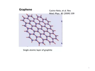
Graphene http://en.wikipedia.org/wiki/Graphene
Tight-binding Model Y. Zhang and R.Tsu, Nanoscale Research Letters Vol. 5 Issue 5 • pz orbital is well separated in energy from the sp2orbitals • More importantly, only the pz electron is close to the Fermi level • Therefore, the common tight-binding method for graphite/graphene considers only the pz orbital (P.R. Wallace, PRB 1947) 2pz 2px 2py 2pz sp2 2s
Passivation in PD and Pz tight binding model • NEMO5: two models for Graphenebandstructure • Standard model of tight binding literature “Pz” • Includes just one pZ orbital per atom • Does not allow for hydrogen passivation • Because pz orbital of C has zero coupling to s orbital in H pZ • Recently developed model “PD” (J. Appl. Phys. 109, 104304 (2011) • Includes {pzdyzdzx} orbital set on each C atom and H atom • Hydrogen atoms included explicitly (realistic treatment) “passivate_H” not required in job_list BUT Make H atoms “active”, i.e. include them explicitly: Domain { activate_hydrogen_atoms = true (default = false) dzx pZ dyz Always have passivate = true in the domain section (default)
Graphene: Primitive Basis a0= 0.142nm A1 a1 K M Γ a2 A2 Lattice basis: Symmetry points: Reciprocal lattice basis: Given in NEMO5 User defined points
Defining the Structure Define the material Dimension in number of unit cells Have “true” only for PD model ‘primitive’ or ‘Cartesian’ With a large enough region, device is limited by dimension only
Defining Solver A1 K M Γ Symmetry points: A2 ‘Pz’ or ‘PD’ Γ K M Γ Expressed in units of A1 and A2
GrapheneBandstructure: PZ vs. P/D NEMO5 Boykin et al. pz p/d DFT results are much better reproduced with the PD model J. Appl. Phys. 109, 104304 (2011)
GrapheneNanoribbons Z.Chen, et al.Physica40, 228-232 (2007)
Graphene: Cartesian Basis A2 a0= 0.142nm a1 A1 a2 Reciprocal lattice basis: Lattice basis: Γ
Structure a1 cartesian a2 A2 A1
Example 1 : 10-AGNR “Armchair” 10 atomic layers wide x Periodic y A big domain
10-AGNR Bandstructure bandgap Armchair edges allow opening up a bandgap
“zigzag” • Exercise: Define a “10-ZGNR” in NEMO5 and calculate its bandstructure along x direction ([100]) a1 y x 1 a2 2 3 a0= 0.142nm 4 9 10
Exercise1 : 10-ZGNR “zigzag” 1 2 3 4 y x 9 10
Bandstructure: 10-ZGNR Zigzag edges give metallic behavior
GrapheneNanomeshes http://today.ucla.edu/ J. Baiet al. Nature Materials 5, 190-194 (2010)
Example 2: GrapheneNanomesh 12 unit cell 7 unit cell Region 1 defines the graphenesupercell 12 unit cell Region 2 defines a hole Only include region 1 in the domain Higher priority in the hole region
Bandstructure: GNM 12 unit cell 7 unit cell Eg = 0.75 eV 12 unit cell Flat bands in the middle of the bandgap Need to visualize the wavefunction at the Γ point
Wavefunction Visualization A new directory That stores all wavefunction files
GNM: Edge state d = 7 uc Propagating state Localized state zigzag High Wavefunctions on the flat band are localized at the zigzag edges Low
Exercise 2: GrapheneNanomesh Exercise: • Define a graphenenanomesh of 8nm x 8nm with rectangular hole 7nm x 1nm. • Plot bandstructure along x and y. • Obtain and visulizewavefunctions at Γ point 8nm a1 1nm y 7nm x 8nm a2 a0= 0.142nm
Exercise 2: GrapheneNanomesh 8nm Structure: 1nm 7nm 8nm
Bandstructure and Wavefunctions High [010] [100] Low Edge state at the zigzag edges