Download
1 / 20
260 likes | 845 Vues
Design of Lateral MOSFET in Silicon Carbide. DESIGN OF LATERAL MOSFET IN SILICON CARBIDE. Mississippi State University Department of Electrical and Computer Engineering. Design of Lateral MOSFET in Silicon Carbide. Team Members. Senior Design I - Researched information on Power MOSFETs

E N D
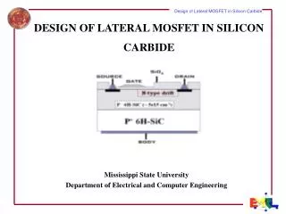
Design of Lateral MOSFET in Silicon Carbide DESIGN OF LATERAL MOSFET IN SILICON CARBIDE Mississippi State University Department of Electrical and Computer Engineering
Design of Lateral MOSFET in Silicon Carbide Team Members • Senior Design I • - Researched information on Power MOSFETs • - Researched information on epitaxial growth methods • - Performed epitaxial growth to determine process • - Project documentation • - Performed SRIM simulations • - Analyzed data from Medici simulations • - Project Website • - Team Page • - Timeline • - Updating Documents • - Determined standard device dimensions • - Created device drawings and cross-sections • - Determine device layers and resulting masks layers • - Worked on mask layout in Cadence • - Project presentations • Senior Design II • - Project Team Leader • - Project documentation • - Project presentations • - Helped with Project Website • - Recorded wafer appearance before and after Silane Anneal • - Helped extract sizes of single finger device • - Performed Blocking Voltage tests for device • - Speaker for final Design Review • Senior Design I • - Project Team Leader • - Researched information on Power MOSFETs • - Performed calculations for On-Resistance • - Performed calculations for Contact Resistance • - Project documentation • - Project presentations • - Project Website • - Title Page • - Abstract • - Updating Documents • - Speaker for Preliminary Design Review • - Speaker for Final Design Review • Senior Design II • - Project documentation • - Helped extract size of single finger devices • - Project presentations • - Helped with Project Website • - Performed Blocking Voltage tests for device Senior Design I- Researched information on power MOSFETs- Project documentation- Researched Cadence design rules for layout - Proofread project documentation- Assisted with web design- Project presentationsSenior Design II- Researched topics on transmission line method (TLM)- Measured contact resistance using TLM - MatLab analysis for contact resistance- Project presentations- Helped with Project Website - Proofread project documentation • Senior Design I • - Research of blocking voltage and associated concepts • - Research of on-resistance in lateral MOSFETs • - Research of contact resistance • - Project documentation • - Project presentations • - Analysis of Medici simulations • Senior Design II • - Project documentation updates • - Further research of Breakdown voltage in SiC devices • - Project presentations • - Speaker for Preliminary Design Review • - Device testing • - Performed Blocking Voltage tests for device Elmer Durrell III Senior - Electrical Engineering ed1@ra.msstate.edu Janna Bonds Dufrene Senior - Electrical Engineering jrb2@ece.msstate.edu Dr. Jeffrey Casady Faculty Advisor Assistant Professor Electrical Engineering Mississippi State University Wendy L. Evans Senior - Electrical Engineering wle1@ra.msstate.edu Christopher R. Sanders Senior - Electrical Engineering crs4@ra.msstate.edu
Design of Lateral MOSFET in Silicon Carbide High Temperature, High Voltage, and High Frequency through Silicon Carbide Technology Brings Dramatic Impacts on Smart Power Applications Military Silicon Carbide MOSFET Commercial • Higher Breakdown Voltage • Lower On-Resistance Consumer
Design of Lateral MOSFET in Silicon Carbide Design Requirements • Epitaxial Layer Growth • Develop and design a repeatable process to grow p-type epitaxy with the dopant concentration between the range of 5e15 cm-3 to 1e16 cm-3. • Fabrication Process • Complete process traveler for the MOSFET fabrication sequence to be executed by the SiC fabrication foundry. • Device Layout • Layout masks used for fabrication of the MOSFETs using Cadence tools, following closely the outlined design constraints. • Blocking Voltage • Devices will be designed to achieve blocking voltages of 600V, 1200V and 1800V.
Design of Lateral MOSFET in Silicon Carbide Design Requirements • On-Resistance • Devices will be designed to have on-resistances of 50mohm-cm2, 350mohm-cm2 and 2450mohm-cm2, for 600V, 1200V and 1800V, respectively. • Contact Resistance • Achieve contact resistance of approximately 1 m - cm2 • Physical Size • Total active area of device will be no larger than 500 m x 500 m. • Cost • Estimated cost to produce and manufacture the set of masks will be approximately $4,000, and four wafers with epi layers will cost approximately $6,000.
SIMULATION SPECIFICATIONS DEVICE SPECIFICATIONS REQUIREMENTS 1-D EXCEL TESTING 2-D SRIM TESTING 2-D MEDICI TESTING CADENCE PROBE STATION Threshold Voltage Fab Process Device Layout Blocking Voltage On-Resistance Contact Resistance Electric Field Physical Size Design of Lateral MOSFET in Silicon Carbide Test Specification
Design of Lateral MOSFET in Silicon Carbide Breakdown Voltage Point A Point B To achieve the minimum degree of breakdown in the gate oxide and silicon carbide, doping was set to Point B - Breakdown of silicon carbide due to low doping in the drift layer. Point A - Breakdown of oxide due to high doping in the drift layer and electric field in the gate oxide. • 2.8E+17 cm-3 in the drift layer • 4.6E+15 cm-3 in the inversion layer
Design of Lateral MOSFET in Silicon Carbide On - Resistance Point A Point C - Channel Resistance - Control doping in inversion layer to limit on-resistance Point C Point A - Drain and Source Resistances - Control doping in the n+ drain and source regions to limit on-resistance To achieve the minimum degree of on-resistance in the device doping was set to • 2.8E+17 cm-3 in the drift layer Point B Point B - Diffusion Resistance - Control doping in diffusion layer to limit on-resistance • 4.6E+15 cm-3 in the inversion layer • 1E+19 cm-3 in the source and drain implant regions
Design of Lateral MOSFET in Silicon Carbide Device Layout Device Layout in Cadence showing size of largest single finger device, which is 83 um x 175 um. Device Layout showing cross-section and lengths (LDR - drift region length, LDFO - drain overlap of field oxide, LPFO - poly overlap of field oxide)
Design of Lateral MOSFET in Silicon Carbide Device Layout in Cadence • Die: • a cell which contains all the devices to be fabricated • arrayed in a pattern to cover a circular region with a 50 mm diameter • Die size: 5 mm x 5mm • Die contains: • 20 single finger devices • 12 ten finger devices • 4 twenty finger devices • Various test structures • Alignment marks
Design of Lateral MOSFET in Silicon Carbide Device Implementation Mask 5: Gate Metal Mask 7: Gate Contact Mask 8: Metal Mask 4: Gate / Field Oxide Mask 6: N Plus Contact Mask 2: N Plus Implant Mask 3: N drift Implant Metal Metal Oxide Oxide Oxide Gate metal N cont Gate Oxide N cont P-type Epitaxy N plus N plus 6H-SiC substrate N drift
Design of Lateral MOSFET in Silicon Carbide Device Implementation Appearance of surface after ion implant and unsuccessful anneal Appearance of surface after ion implant and successful anneal
Design of Lateral MOSFET in Silicon Carbide EXCEL Testing Results 0.02 0.017 1800V 0.015 1200V 0.013 600V 0.01
Design of Lateral MOSFET in Silicon Carbide MEDICI Testing Results Shows that design requirement is obtainable. >600V 2.8E+17
Design of Lateral MOSFET in Silicon Carbide MEDICI Testing Results ~1450V 2.8E+17
Design of Lateral MOSFET in Silicon Carbide MEDICI Testing Results ~1850-1900V 2.8E+17
REQUIREMENTS SIMULATION RESULTS ACTUAL RESULTS OBTAINED OBJECTIVE? BLOCKING VOLTAGE (600, 1200, 1800V) 650, 1450, 1900 N/A ON-RESISTANCE (50, 350, 2450m-cm2) 13, 15, 17 N/A CONTACT RESISTANCE (1m-cm2) 2.32 to 3.4 EPI GROWTH (5e15 to 1e16cm-3) 5 e15 to 1e16 4.6e15 to 1.3e16 PHYSICAL SIZE (500 x 500µm) 500 x 500 66 x 167 COST ($4,000) 4, 000 9,000 Design of Lateral MOSFET in Silicon Carbide Results ? ? 0.6 Yes Yes Yes No More masks were made than planned and smaller critical dimension tolerance was selected.
Design of Lateral MOSFET in Silicon Carbide Future Work • Optimize layouts (gate length, drift length, overlap spacing) based on results from this design • Utilize future advancements in material process technology • Design on a SiCOI (SiC on Insulator) • Continue research in epitaxy growth methods
Design of Lateral MOSFET in Silicon Carbide We would like to give thanks to… * General Electric Corporate Research and Development - Wafer fabrication and Partial funding * Office of Naval Research - Partial funding * EMRL - Providing facilities and SiC research Special thanks to ... * Will Draper - Cadence contributions * Igor Sankin - Medici contributions * Dr.Steve Saddow - Annealing Process
Design of Lateral MOSFET in Silicon Carbide DESIGN OF LATERAL MOSFET IN SILICON CARBIDE Mississippi State University Department of Electrical and Computer Engineering