Lab 4: FPGA Implementation
Why Top-Down?. Design of complex systemsReduce time-to-marketshorten the design verification loopfocus on functionalityEasier and cheaper to explore different design option. RTL Design. Characteristicsfully clock driven RTL code with some behavioral constructscontain complete functional descriptioncycle accurateCoding stylestructural description (component connections/net-list)data flow description (continuous assignment)RTL description (always block)combinational RTLsequential RTL.273
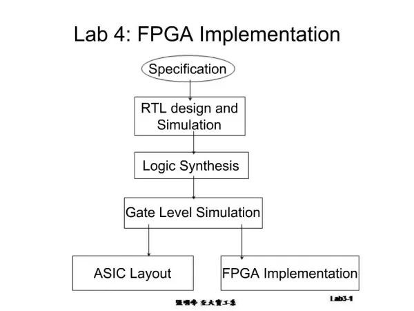

Lab 4: FPGA Implementation
E N D
Presentation Transcript
1. Lab 4: FPGA Implementation
2. Why Top-Down? Design of complex systems
Reduce time-to-market
shorten the design verification loop
focus on functionality
Easier and cheaper to explore different design option
3. RTL Design Characteristics
fully clock driven RTL code with some behavioral constructs
contain complete functional description
cycle accurate
Coding style
structural description (component connections/net-list)
data flow description (continuous assignment)
RTL description (always block)
combinational RTL
sequential RTL
4. Logic Synthesis Translate synthesizable RTL code to gate-level design
5. Structural Mapping
6. Resource Sharing Example
if (op_code ==0)
r = a + c ;
else
r = a + b ;
Sharing
a single ALU for the two additions
a MUX for the second input of the ALU
No-Sharing
two adders for the two additions
an output MUX to select the output
7. Register Inferencing Determines which signals must be preserved across cycle boundaries
incomplete logic specification (missing branches)
explicit register instantiation
always @(posedge clk)
signal used before assigned
8. Two-level Logic Optimization AND-OR representations
easy implementation as PLAs and PLDs
a key optimization technique
efficient algorithms and heuristics exist
in commercial use for several years
minimize the number of product terms
Example
F = XYZ + XY�Z� + XY�Z + X�YZ + XYZ
F = XY� + YZ
9. Multi-Level Logic Optimization Meet performance or area constraints through restructuring and simplifications
two-level minimization
common factor extraction
common expression resubstitution
Trade-off between area and delay
In commercial use for several years
f1 = abcd+abce+ab�cd�+ab�c�d+a�c+cdf+abc�d�e�+ab�c�df�
f2 = bdg + b�dfg + b�d�g+bd�eg
f1 = c(a�+x)+ac�x�
f2 = gx
x = d(b+f) + d�(b�+e)
10. Technology Mapping Translation of a technology independent representation of a circuit into a circuit in a given technology with optimal cost
Optimization criteria
minimum area
minimum delay
meeting specified timing constraints
meeting specified timing constraints with minimum area
Usages
Technology mapping after technology independent logic optimization
11. Sample covers
12. State Machine Synthesis Translate state table or graph
state minimization
state assignment to minimize the cost function
Challenges
state machine decomposition
state assignment for performance
state assignment for testability
extract state graph from implementation
13. Spartan II Features Plentiful logic and memory resources
15K to 200K system gates (up to 5,292 logic cells)
Up to 57 Kb block RAM storage
Flexible I/O interfaces
From 86 to 284 I/Os
16 signal standards
Advanced 0.25/0.22um 6-Layer Metal Process
High performance
System frequency as high as 200 MHz
Advanced Clock Control with 4 Dedicated DLLs
Unlimited Re-programmability
Fully PCI Compliant
Spartan FPGAs provide the low cost and high feature content required to be used in consumer electronics applications.Spartan FPGAs provide the low cost and high feature content required to be used in consumer electronics applications.
14. Spartan-II Top-level Architecture Configurable logic blocks
Implement logic here!
I/O blocks
Communicate with other chips
Choose from 16 signal standards
Block RAM
On-chip memory for higher performance Now we will look at the details of the architecture. Each of these sections will be examined in more detail later in the presentation.Now we will look at the details of the architecture. Each of these sections will be examined in more detail later in the presentation.
15. Spartan-II Top-level Architecture Clocks and delay locked loops
Synchronize to clock on and off chip
Rich interconnect resources
Three-state internal buses
Power down mode
Lower quiescent power
16. CLB Slice (Simplified) 1 CLB holds 2 slices
Each slice contains two sets of the following:
Four-input LUT
Any 4-input logic function
Or 16-bit x 1 RAM
Or 16-bit shift register The FPGA is made up of an array of Configurable Logic Blocks (CLBs), and each CLB is made up of two slices, and each slice has two Look-Up Tables (LUTs) and 2 flip-flops.The FPGA is made up of an array of Configurable Logic Blocks (CLBs), and each CLB is made up of two slices, and each slice has two Look-Up Tables (LUTs) and 2 flip-flops.
17. CLB Slice (cont�d) Each slice contains two sets of the following:
Carry & control
Fast arithmetic logic
Multiplier logic
Multiplexer logic
Storage element
Latch or flip-flop
Set and reset
True or inverted inputs
Sync. or async. control
18. Dedicated Expansion Multiplexers MUXF5 combines 2 LUTs to form
4x1 multiplexer
Or any 5-input function
MUXF6 combines 2 slices to form
8x1 multiplexer
Or any 6-input function Special logic in the CLB allows logic expansion beyond just using the lookup tables.Special logic in the CLB allows logic expansion beyond just using the lookup tables.
19. I/O Block (Simplified) Registered input, output, 3-state control
Programmable slew rate, pull-up, pull-down, keeper and input delay The I/O block features are automatically used according to the design entered into the development system.The I/O block features are automatically used according to the design entered into the development system.
20. I/O Interface Standards I/O can be programmed for 16 different signal standards
VCCO controls maximum output swing
VREF sets input, output, three-state control
Different banks can support different standards at the same time
Logic level translation
Boards with mixed standards
A wide variety of I/O interface standards are supported, such as HSTL, SSTL, GTL, etc.A wide variety of I/O interface standards are supported, such as HSTL, SSTL, GTL, etc.
21. IOBs Organized As Independent Banks As many as eight banks on a device
Package dependent
Each bank can be assigned any of the 16 signal standards
22. High Performance Routing Hierarchical routing
Singles, hexes, longs
Sparse connections on longer interconnects for high speed
Routing delay depends primarily on distance
Direction independent
Device-size independent
Predictable for early design analysis The development system automatically takes advantage of abundant routing to implement any design quickly and efficiently. Timing does not vary considerably from one implementation to the next since delays are based on distance, not direction.The development system automatically takes advantage of abundant routing to implement any design quickly and efficiently. Timing does not vary considerably from one implementation to the next since delays are based on distance, not direction.
23. Power-down Mode Controlled by single power down pin
All inputs blocked, appear low internally
All outputs disabled
All register states preserved
Power-down status pin
Synchronous wake up
100 uA typical A dedicated Power Down pin helps conserve the power resources.A dedicated Power Down pin helps conserve the power resources.
24. Configuration Modes The user can choose the configuration mode that best suits the particular application.The user can choose the configuration mode that best suits the particular application.
25. Spartan-II Family Overview The XC2S200 was recently added to extend the family to 200,000 system gates.The XC2S200 was recently added to extend the family to 200,000 system gates.
26. Spartan-II Architecture Summary Delivers all the key requirements for ASIC replacement
200,000 gates
200 MHz
Flexible I/O interfaces
On-chip distributed and block RAM
Clock management
Low power
Complete development system support
27. Design Tools Standard CAE entry and verification tools
Xilinx Implementation software implements the design
The design is optimized for best performance and minimal size
Graphical User Interface and Command Line Interface
Easy access to other Xilinx programs
Manages and tracks design revisions
28. Foundation Project Manager Integrates all tools into one environment
29. Schematic Entry
30. ABEL, Verilog and VHDL Text Entry From schematic menu (or via HDL Editor), select Hierarchy -> New Symbol Wizard� to create symbol.
Select HDL Editor & Language Assistant to learn by example, then define block.
Synthesize to EDIF.
31. State Machine Graphical Editor
32. Simulation - Easy to Use and Learn
33. What is Implementation? More than just �Place & Route�
Implementation includes many phases
Translate: Merge multiple design files into a single netlist
Map: Group logical symbols from the netlist (gates) into physical components (CLBs and IOBs)
Place & Route: Place components onto the chip, connect them, and extract timing data into reports
Timing (Sim): Generate a back-annotated netlist for timing simulation tools
Configure: Generate a bitstream for device configuration
34. Terminology Project
Source file; has a defined working directory and family
Version
A Xilinx netlist translation of the schematic
Multiple Versions result from iterative schematic changes
Revision
An implementation of a Xilinx netlist
Multiple revisions typically result from different options
Part type
Specified at translation; can be changed in a new revision
35. Starting the Flow Engine
37. XSA-50 Board Xilinx XC2S50
7-seg LED
100 MHz prog. osc.
SDRAM
8M*8
Flash
128K bytes
XC9572XL
Parallel port
PS/2 port
VGA port
38. Xstend Board 2 7-seg LED
Bargraph LED
Dip switch
Pushbuttons
Stereo Audio I/O
RS-232
USB 1.1
39. Lab 4: 7-Segment Decoder input [3:0] sig ; // 0-F
output [6:0] control ; // active high
40. 4-bit Magnitude Comparator input [3:0] a, b ;
input agb, alb, aeb ;
11 input pins
XSTend Board S1
XSA-50 board SW1
41. 4-bit Magnitude Comparator output agbo, albo, aebo ;
Use XSTend Board
Bar LEDs