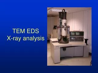
TEM EDS - Analysis Precautions
TEM EDS - Analysis Precautions. Analysis Precautions. You need to think more about experimental conditions in TEM/STEM than in SEM. Spatial resolution is strongly affected by experimental conditions in TEM/STEM. Spurious X-rays are a significant issue in TEM/STEM.

TEM EDS - Analysis Precautions
E N D
Presentation Transcript
Analysis Precautions • You need to think more about experimental conditions in TEM/STEM than in SEM. • Spatial resolution is strongly affected by experimental conditions in TEM/STEM. • Spurious X-rays are a significant issue in TEM/STEM
What do you need to think about? • Illumination system issues • Sample and stage issues • Detector issues • Specimen preparation issues
Pt Obj aperture TEM EDS geometry
Illumination issues • Spherical aberration • Hard X-rays • Hole count
Spherical Aberration Large fraction of electrons are outside of the FWHM and will generate x-rays FWHM is what your eye will see
Aberrated electrons • More of an issue in nano-probe mode. • Choose the optimum C2 aperture to limit spherical aberration. More beam current is not necessarily better.
Hard X-rays • Bremsstrahlung is generated whenever electrons are slowed down. (e.g. hitting condenser apertures) • TEM/STEM will have bremsstrahlung up to 200 keV compared to ~30 keV in SEMs.
Identifying hard X-rays • Use a hole-count test. • X-rays have a smaller ionization cross-section than electrons, therefore more of an effect in “bulk” areas than in “thin” areas. • Ionization occurs deeper in sample, thus low energy lines are preferentially absorbed.
Hard X-Ray Mitigation • Thicker apertures will reduce hard X-Rays (“Top Hat” apertures). Do not use Au “thin-foil” apertures • On FEG instruments use the adjustable C1 aperture as the beam limiter and use C2 as a “spray” aperture.
Sample and stage issues • Scattered electrons • Continuum radiation • BSE
Pt Obj aperture Scattered electrons and BSE
Stray scattered electrons • BSE coefficient is ~0.3 for Fe and Cu (~0.7 for Pt) • Lens design can help if the post-field keeps large angle electrons within lower bore… … IF you remove the Objective aperture.
Sample self-fluorescence • The bremsstrahlung as the electrons go through the sample will be a forward scattered “dipole” (relativistic effects). • Tilted samples (particularly thinned foils) may receive a sizeable dose of sample generated hard X-rays. • Grid bars may also fluoresce.
Trapped BSE • This is a function of the BSE coefficient and thickness. Pt caps on FIB samples may backscatter stray electrons. • This may be more of an issue with thinned samples.
Absorption edges • Visible in thick samples (grid bars, etc.) • Makes it difficult to fit continuum background.
Source of stray signal • High L/K ratio indicates electron rather than X-ray excitation • Absorption edges in the high energy peaks indicate the source is in a thick area.
Electron channeling • In a strong diffracting condition, the electrons can preferentially excite certain columns of atoms. • This can lead to misleading compositions. • It can also be used to observe atom locations. (ALCHEMI)
Detector issues • BSE detection and damage • Detector Efficiency issues • Detector icing • Escape and sum peaks • Incomplete charge collection
High energy BSE • Will affect system dead-time calculations esp. if variations in Z across sample. • Will affect peak shape and hence intensity calculations • Will cause damage (point defects) to the detector resulting in incomplete charge collection (low energy tails on peaks).
Sample and preparation issues • Sample issues • Surface films • Ar+ and Ga+ implantation
Considerations • FIB samples are thin enough that you should not see significant contributions from hard X-rays (within the sample). • Watch out for sample contamination with small probes. Plasma-clean thinned samples and/or use a cryo-stage. Pre-heating the sample helps too. • Extraction replicas may provide a means to analyze precipitates without matrix interference. • Consider a tilt-rotate holder for looking at interfaces.
SEM Standardless EDS Sample: 123 Superconductor Compositions in Wt %
SEM Standardless EDS Sample: 123 Superconductor Compositions in Wt %
SEM Standardless EDS Sample: 123 Superconductor Compositions in Wt %
SEM Standardless EDS Sample: 123 Superconductor Compositions in Wt % Moral: Be careful about standardless analysis. You can get almost any result you want!
EDS Resources • Monte Carlo simulations • Casino • WinXRay • DTSA and DTSA-II • http://www.cstl.nist.gov/div837/Division/outputs/DTSA/DTSA.htm • DTSA - Macintosh (not OS-X) only • DTSA-II - Java • www.oxinst.com – “TEM Explained.pdf”
Next week • Sample preparation • Specific questions? • Course evaluation • I’ll send link when I get it. • Practical exam scheduling • CM12 alignment • Diffraction (spot and k-line) • Sample tilting, BF/DF
Laboratory 8 • Sample: NiOx thin film on a Mo grid • Hole count in microprobe mode • Electron spectrum of grid • Nano-probe EDS with large and small C2 aperture • EDS at large and small a-tilt angles