Sid
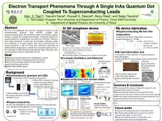
Electron Transport Phenomena Through A Single InAs Quantum Dot Coupled To Superconducting Leads Hsin Z. Tsai a,b , Yasushi Kanai b , Russell S. Deacon b , Akira Oiwa b , and Seigo Tarucha b NanoJapan Program, Rice University and Department of Physics, Texas A&M University

Sid
E N D
Presentation Transcript
Electron Transport Phenomena Through A Single InAs Quantum Dot Coupled To Superconducting Leads • Hsin Z. Tsaia,b, Yasushi Kanaib, Russell S. Deaconb, Akira Oiwab, and Seigo Taruchab • NanoJapan Program, Rice University and Department of Physics, Texas A&M University • Department of Applied Physics, the University of Tokyo Sid • Abstract • We aim at investigating the quantum transport through an InAs self-assembled quantum dots (SAQD) coupled with superconducting leads. We will show results of electrical transport through a single QD coupled with Al leads. Transports specific for superconductivity, quasiparticle tunneling and Andreev reflection have been observed. In particular, the Andreev reflection peaks are enhanced in Kondo regime. We have characterized the superconductivity of Nb thin films and nanowires deposited by electron-beam evaporator to realize the enhanced supercurrent in the new type of InAs SAQD devices with Nb leads. We have done the preparation works of making Nb devices. • Goal • Observe proximity supercurrent (Josephson current) • Side gate control of the supercurrent in Al device • Study of the interplay between Kondo effect and superconductivity phenomena • Realize Nb/InAs/Nb system • Al QD Josephson device • Uncapped InAs SAQD: Diameter ~ 80nm, Height ~ 20nm • Gap size ~30nm, in plane sidegate is100nm from gap • Superconducting electrodes ( thickness Ti/Al : 5/100 nm) • - Critical temperature Tc ~ 1.2K • - Critical magnetic field Bc ~ 120mT • Source-drain biased: controlled by the voltage cross the lead • Nb device fabrication • Superconducting Nb thin film evaporation • Evaporate pure Nb to GaAs wafer and test its superconductivity (Tc~9.25k) • Tc~2.5K Ti/Al 200nm InAs dot • At 2.5K, the resistance suddenly drop to zero • Ic ~3mA at 2.409K Sidegate Device crossection SEM Image • Nb lead fabrication and • The pattern of the nanowire is made by electron beam lithography • Evaporate Nb/Ti on the e-beam resist and lift off the extra part Nanowire • By the similar method, we • make Nano gap between • superconducting Nb nanowire 20nm Nano Gap • Coulomb Oscillation and Diamond 200nm 300nm T ~ 50 mK B ~ 200 mT Charging energy Ec ~ 3 meV • Test the superconductivity through gold pad, 4-termnal measurement Current -0.3 0.3 0.6 0 Vg(V) e/h 4 • Background • Semiconductor quantum dot (QD) • 1. Small size of QD quantize energy level • 2. When Fermi energy of the lead • match the energy level in • the dot, the electron can • transport through the dot. • 3.Gate voltage can tune the • dot energy level and coulomb • oscillation occur Vsd(mV) 0 Kondo effect -4 • Superconducting and normal states Superconducting state Normal state • Superconducting gap • D ~ 150 meV • Quasi-particle tunneling • Andreev reflection • Kondo regime • Andreev reflection peaks are enhanced • Summary & Conclusion • We measured the transport though the single InAs self-assembled QD coupled to Al leads • Superconducting transports were observed but the supercurrent could not be measured due to the weak coupling • We have tested the Nb deposition using EB evaporator and prepared the Nb thin films and nanowires • Some of the films could have critical temperature at 2.5 K at most 2D:quasiparticle tunneling Ic~5mA D: Andreev reflection Kondo effect Sidegate effect Change in conductance in Kondo valleys by sidegate Andreev transport and Kondo effect? • Superconductivity • At very low temperature, two electrons form a Cooper pair and zero resistance state appears in the material -2D -D +D +2D • Future works • Improve the superconductivity of the Nb thin film • Complete Nb/InAs/Nb device and test the electron transport with higher critical current • Study the interplay between Kondo effect and superconductivity using the side gate effect • Josephson Junction • - Cooper Pair tunneling • - Supercurrent This work was supported by the National Science Foundation under Grant No. OISE‐0530220. s I s phonon Cooper pair http://nanojapan.rice.edu Josephson Junction