Comprehensive Performance Evaluation of PROCStar III FPGA Board for Optimal Design Strategies
In this semestrial project, we investigate the performance characteristics of the PROCStar III Stratix III 260E FPGA board, focusing on optimizing design strategies for future users. Our goal is to create various tests to analyze the board's communication channels, internal and external memory transfer rates, and overall processing capabilities. Specific tests include evaluating internal memory transfer rates, external memory bandwidth, FPGA-to-FPGA communication, and executing mathematical operations. The insights from these tests will provide students with vital information for efficient project planning.

Comprehensive Performance Evaluation of PROCStar III FPGA Board for Optimal Design Strategies
E N D
Presentation Transcript
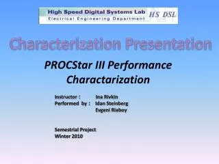
Characterization Presentation PROCStar III Performance Charactarization Instructor:Ina RivkinPerformed by:Idan Steinberg EvgeniRiaboy Semestrial Project Winter 2010
Overview • With the introduction of a new FPGA based board, we have to devise a series of tests to examine the devices max practical performance, allowing the students that use these boards for future projects, to plan optimal design based on the concluded tested performance.
Goals Devising Different Tests to examine the performance of the board: • Communication testing between: • PCI channel ↔ on chip memory • PCI channel ↔ off chip memory (external DDR memories) • FPGA’s • Checking performance of on chip recourses • Concluding the optimal working recommendations for the PROCStar III 260E Board
GidelPROCstar III Stratix III 260E • 4 AlteraStratix III 260E FPGA’s, with 256 MB on chip memory • 8 Lane PCIe host interface • 8 DDR2 Banks, with 2*2GB on first FPGA, and 1*2GB on the other FPGA’s • ~2MB FPGA Internal RAM • 255K Logic Elements (per FPGA)
Project Plan Test 1: Internal Memory Transfer Rate: • We will fill the internal memory with data, and read it back, thus determining the transfer rate. Procstar III Stratix III Internal memory PCIe Controller (DMA Mode) PCIe
Project Plan Test 2: External Memories Transfer Rate: • We will fill the memory (testing each bank A, B, C separately) with data, and read it back, thus determining the transfer rate for each memory, both in Multi FIFO and Multi Port Configurations. Procstar III A Stratix III PCIe Controller (DMA Mode) B PCIe C
Project Plan Test 3: FPGA Communication: We will read data from an internal memory on one FPGA and transfer it to an adjacent FPGA on their direct connection and write it to the second FPGA’s internal memory.
Project Plan Test 4: FPGA Communication: We will read data from an internal memory on one FPGA and transfer it to all other FPGA’s on their local BUS connection and write it to their memories
Project Plan Test 5: Internal Functions Testing: We will perform different mathematical operations: • Add • Subtract • Multiply – both in LE and in DSP blocks • Divide • Sqrt For fixed point and floating point operations, determining the DSP and LE performance.
Preparing simple examplefor the midterm presentation: An example with the usage of the required resources for the main project plan – taking data from the PCI, writing it to the internal FPGA memory, performing mathematical operation and writing it to a DDR: PCIe Internal Memory Mathematical Operation PCIe DDRin Multi Port Memory