Download
1 / 21
220 likes | 590 Vues
Explore direct/indirect bandgaps, electron-hole interactions, E-k relationships, and density of states in semiconductors like Silicon, GaAs, and Germanium. Learn about semiconductor band diagrams and Fermi distribution functions.

E N D
Band structure in semiconductors: Direct/indirect bandgaps Density of states Electrons and Holes E-k relationships for: Silicon GaAs Germanium Lecture 2: Electrons in semiconductors I Semiconductor Applications L2
Semiconductor band diagram Fermi distribution function Carrier concentration Reminder of Lecture 1 Concepts Semiconductor Applications L2 Density of states Density of allowed states per energy range
A solution of the Schrödinger equation provides an energy versus effective momentum E-k relationship. This is called the band structure of the semiconductor. In semiconductor physics, we are interested in the properties of the E-k relation near the top of the valence band and the bottom of the conduction band. Band structure of semiconductors Semiconductor Applications L2
The top of the valence band occurs at k=0 in most semiconductors. Notice the presence of two different E-k curves near the valence band edge, labelled the Heavy Hole and Light Hole bands. The bottom of the conduction band in some semiconductors occurs at k=0. Such semiconductors are called directbandgap semiconductors. Examples include, GaAs and InP If the bottom of the conduction band does not occur at k=0, the semiconductor is termed indirect. Examples include Si and Ge. The alignment of the valence and conduction bandedges has important consequences. Direct bandgap semiconductors have a strong interaction with light. This is a result of the law of momentum conservation. Band structure of semiconductors Semiconductor Applications L2
When the conduction bandedge is at k=0, the band structure can be represented by: EC is the conduction bandedge, and the band structure is a simple parabola. Notice that the E-k relation looks like that of an electron in free space except that the free electron mass m0 is replaced by the effective mass m*. The electron responds to the outside world as if it had this mass, of course the real electron mass does not change. The conduction band electron effective mass has a strong dependence on the bandgap, the smaller the bandgap the smaller the effective mass. Direct bandgap semiconductors Semiconductor Applications L2
In silicon the bottom of the conduction band occurs at six equivalent minima along the x, y and z-axis. The k values at the minima are: And their inverses, where a (lattice constant) is 0.543nm for Si. For each of the six k points the conduction-band energy reaches a minimum value and as k moves away from these values the energy rises. These valleys in the conduction band have the energy momentum relationship: For valleys along the x-axis and –x-axis. m*l longitudinal effective mass 0.98m0. m*t transverse effective mass 0.19m0 Indirect bandgap semiconductors Semiconductor Applications L2
The particle momentum for a free electron is zero when the kinetic energy is zero. An electron at the conduction band minimum can have crystal momentum different from zero. In silicon when an electron makes a transition from the valence band to the conduction band, it requires not only an energy change but also a change in crystal momentum. Indirect bandgap semiconductors • What does this mean? • The fact that the minimum in the conduction band does not occur at k=0 illustrates the main difference between particle momentum and crystal momentum. Semiconductor Applications L2
The E-k relationships near the minimum of the conduction band or the maximum of the valence band are parabolic as indicated by: With a well known E-k relationship, the effective mass can be obtained from the second derivative of E with respect to hk: Therefore the narrower the parabola, the smaller the effective mass. GaAs has a very narrow conduction band parabola and the electron effective mass is 0.07m0. For silicon it is 0.19m0 ([100]-direction). E-k relationships Semiconductor Applications L2
Using effective mass instead of electron mass we can obtain a value for the density of states. Assuming an E-k relationship of the form: The conduction band density of states becomes: For indirect bandgap semiconductors, the conduction band density of states mass used in the above expression is: For the valence band the density of states is: This is zero for E>Ev Semiconductor DOS – Conduction Band Semiconductor Applications L2
The energy-momentum relationship in the valence band is: for the heavy hole and light hole bands respectively. The valence band density of states is hence: The density of states mass for the valence band is given by: Semiconductor DOS – Valence band Semiconductor Applications L2
Calculate the k-value for an electron in the conduction band of GaAs with energy 0.1eV. Compare this to the case of an electron in free space. For GaAs the appropriate mass in the conduction band is 0.067m0: In free space the value is: The two values are different since the k-value in the crystal represents the effective momentum. Example calculation: k-values Semiconductor Applications L2
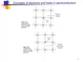
At finite temperatures electrons are promoted from the valence band to the conduction band. The valence band is left with unoccupied states. The concept of holes is introduced as a fictitious mathematic construction. It carries a positive charge and moves under the influence of an applied electric field, in a direction opposite to that of an electron. Mathematically, when all the valence band states are occupied, the sum over all wavevector states is zero: This says there are as many positive k states occupied as negative. In a situation where the electron at wavevector ke is missing, the total wavevector is Holes in semiconductors Semiconductor Applications L2 hole
As indicated previously. At finite temperatures electrons are promoted from the valence band to the conduction band. The combination of the electron and hole is termed an electron-hole pair. It is roughly the solid-state analogue of the ion pair in gases. The probability per unit time that an electron-hole pair is generated is given by: T is the absolute temperature, Eg is the bandgap energy, kB is the Boltzmann constant and C is a proportionality constant characteristic of the material. Electron-hole pairs Semiconductor Applications L2
In the absence of an external electric field the created electron-hole pairs will recombine. An equilibrium is established in which the concentration of electron-hole pairs observed at any time is proportional to the rate of formation. This equilibrium concentration is a strong function of temperature and will decrease drastically if the material is cooled. Electron-hole pairs Semiconductor Applications L2
Relatively easy to fabricate Excellent processing properties High-quality native oxide Bandgap is 1.1eV Has poor optical properties Band structure of Silicon Semiconductor Applications L2
Superior electronic bandstucture to Si Does not have an oxide Difficult to process Excellent optical properties Bandgap is 1.43eV at 300K Sharp bandedge Room temperature semiconductor Band structure of GaAs Semiconductor Applications L2
Germanium is an indirect semiconductor Bottom of conduction band occurs at 8 points. Hole properties of Ge are best of any semiconductor (low hole masses). Was the semiconductor of choice. Processesing considerations. Bandgap 0.9eV means that Ge must be cooled. Material of choice for gamma-ray based radiation detectors. Band structure of Ge Semiconductor Applications L2
Properties of semiconductors Semiconductor Applications L2 A selection of important semiconductor properties
At room temperature, the values of the bandgap are 1.12eV for silicon and 1.42eV for gallium arsenide. The bandgap approaches 1.17eV for Si and 1.52eV for GaAs at 0K. The variation with temperature can be expressed for Si: For GaAs Properties of semiconductors Semiconductor Applications L2
Calculate the effective momentum of an electron in the conduction band of GaAs when the electron energy measured from the bandedge is 0.5eV. E-k relation is m*=0.067m0: The effective momentum is hence: Free electron momentum Example: Effective momentum Semiconductor Applications L2
Bandstructure in semiconductors: Direct/indirect bandgaps Density of states Electrons and Holes E-k relationships for: Silicon GaAs Germanium Summary of Lecture 2 Semiconductor Applications L2