Design of SEU-Robust Configurable Logic Blocks for Radiation-Tolerant FPGAs
This paper presents the development of a radiation-tolerant, Single Event Upset (SEU)-robust reprogrammable FPGA using CMOS 0.25 μm technology. We designed a user-configurable logic block capable of implementing any Boolean expression with four variables. By minimizing the risk of single event transients in combinatorial logic and using SEU-robust registers, the design achieves significant immunity to radiation effects. A test chip comprising 32 logic blocks was fabricated and tested in a heavy-ion beam facility, demonstrating robustness against radiation up to an LET of 79.6 cm²MeV/mg.

Design of SEU-Robust Configurable Logic Blocks for Radiation-Tolerant FPGAs
E N D
Presentation Transcript
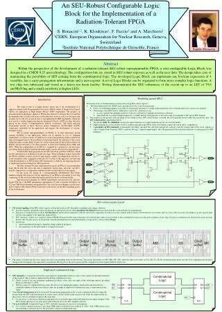
An SEU-Robust Configurable Logic Block for the Implementation of a Radiation-Tolerant FPGAS. Bonacini1,2, K. Kloukinas1, F. Faccio1 and A. Marchioro11CERN, European Organization for Nuclear Research, Geneva, Switzerland2Institute National Polytechnique de Grenoble, France Sandro Bonacini Abstract Within the perspective of the development of a radiation-tolerant SEU-robust reprogrammable FPGA, a user-configurable Logic Block was designed in a CMOS 0.25 μm technology. The configuration bits are stored in SEU-robust registers as well as the user data. The design takes care of minimizing the possibility of SET coming from the combinatorial logic. The developed Logic Block can implement any boolean expression of 4 variables, has a carry propagation infrastructure and a user-register. A set of Logic Blocks can be organized to form more complex logic functions. A test chip was fabricated and tested in a heavy-ion beam facility. Testing demonstrated the SEU robustness of the circuit up to an LET of 79.6 cm2MeV/mg and a small sensitivity at higher LETs. • Hardening against SEUs • Protection of the stored information is achieved by using SEU-robust registers: • The Dual Interlocked Cell (DICE) latch, introduced in [9] is a good starting point • It has a 2×-redundand memory loop and it is intrinsically insensitive to single-node particle hits on its network when static (closed, not clocked). • Nevertheless, the DICE latch is vulnerable if one of two conditions occur: • in case a particle hits multiple nodes, an event also referred to as multiple node charge collection; • when the latch is clocked at high frequencies (>1 GHz) and the clock period is of the same order of magnitude of the typical SEU duration. • The registers in the present work are made of two identical basic SEU-robust latches cascaded, the first being the master, while the second the slave. The SEU-robust latch is represented below. • The latch is Fully 2×-redundant, having two input terminals, two output terminals and two local clock-buffers. • Duplicating the local clock buffer avoids a weakness present in the DICE: if the clock buffer is upset, the whole cell is compromised. • A possibility of SET immunity is introduced: the buffer can upset the cell if the particle hit coincides with the closing edge of the clock, which is a typical Single Event Transient (SET) condition. Having 2 separate input/outputs, the cell represented below provides therefore a starting point for SET immunity. Introduction This work is part of a bigger project whose aim is the development of a radiation-tolerant Field Programmable Gate Array (FPGA) robust to Single Event Upsets (SEUs) for application in High Energy Physics (HEP) experiments. The progress in microelectronic technologies applied to FPGAs has allowed to decrease the costs and the development time of digital electronics in the industrial sector as well as in the space and avionics sector. The use of such devices is also appealing for HEP experiments, which are now forced to exploit Application-Specific Integrated Circuits (ASICs) in their detectors placed in the vicinity of high-luminosity particle accelerators. The harsh radiation environment present in these detectors makes Commercial Off-The-Shelf (COTS) components unsuitable for the application and requires the development of custom-designed circuits. The in-system reprogrammability of FPGAs is of great importance giving extreme flexibility to the application, which can be updated in case of changing requirements or failure recovery. In addition, in-circuit reprogramming reduces further the logic development time by the possibility of observing directly the operation of the circuit within the target system. Many studies [1], [2] have been done on the radiation effects on FPGAs and proved them to be often sensitive to both Total Ionizing Dose (TID) and SEUs. When the configuration of an FPGA is corrupted by a particle hit, the user logic can end up being modified, therefore the functionality can be affected and compromised. Solutions have been proposed for the SEU sensitivity problem of FPGAs, which involve introduction of redundancy in the user logic. These techniques reduce drastically the FPGA available circuitry resources and require complex reconfiguration schemes to avoid corruption of the configuration data [3], [4]. Contrary to this approach, our final aim is the development of an FPGA where SEU insensitivity is built-in, not requiring the user to exploit any special technique for SEU protection. The basic element for logic implementation inside an FPGA is a programmable Logic Block (LB) that allows the user to implement various logic functions. An LB is usually composed of a configurable combinatorial block which drives a user register. In this work, the design of a reprogrammable SRAM-based SEU-robust radiation-tolerant LB necessary for the realization of an FPGA is presented. A test chip comprising 32 LBs has been fabricated and irradiated in a heavy-ion beam facility. Special layout techniques for CMOS technologies were proven to be effective against TID up to the HEP experiments requirements [5] and a standard cell library in 0.25 μm CMOS was designed and qualified [6]. The same layout techniques can be easily used to make a TID-tolerant FPGA, hence this work focuses on the SEU hardening aspect of the development. SEU-robust register layout • The circuit topology of the SEU-robust register used in this work is still vulnerable to multiple node charge collection • In order to protect against this upset mechanism, an appropriate layout which maximizes the distance between sensitive nodes of the network was implemented. • This goal is attained in the layout by interleaving the master latch components with the slave latch components in such a way that a master node is always in between two slave nodes and vice versa. The two local clock buffers are also spaced apart and the same applies to the input and output buffers. • SEU sensitivity studies on a radiation-tolerant SRAM fabricated in the same technology [10] showed that while it was possible to detect multiple-bit upsets in cells with a distance of less than 10 μm, no correlation was observed for errors in more distant cells. For this reason, in the present work the minimum distance between memory storage nodes is always above 10 μm. • Drawbacks: • dense and difficult routing is required to bring signals to far places • the capacitance of the interconnects is slightly increased • The figure is divided into the areas which affect the corresponding nodes in the network. The master latch nodes are MA, MB, MC, MD, while the slave latch nodes are SA, SB, SC, SD. By interleaving the master and the slave components the distance among nodes belonging to the same latch is maximized. The layouts of the user register and the configuration block register differ from this one. • Duplicated combinatorial logic • SET immunity is eventually achieved by providing two independent identical copies of the signals for the input terminals of the registers. This is done by duplicating the driving combinatorial logic. • Upsets in one of the two redundant combinatorial blocks affect only one input of the following register, providing therefore robustness to SETs. • The two copies of combinatorial logic must also receive two independent inputs, which will come from the two redundant outputs of the previous register stage. An example of duplicated combinatorial logic is represented in the figure. • Some circuit timing issues must be discussed: the maximum propagation delay of each combinatorial block is logically decreased by the SET expected duration. A correct value is in fact loaded in the registers only if the two inputs match on the correct value for an interval equal to the setup time. • It is necessary to allocate an additional time interval for a possible upset which will make the two inputs disagree. Only SETs shorter than the excess time given will be filtered out by the SEU-immune structure. • The area overhead of duplicated logic is 100%, with the same increase in power consumption. • It is a better solution in terms of area than TMR which would have an overhead of 200%. Still, TMR doesn’t have special timing constraints and it is the preferable solution for high speed logic.
Logic Block structure • The choice of the complexity of the basic LB of an FPGA is a trade-off between the necessary routing resources and utilization efficiency. • Studies [15] showed that a 4-input-1-output LB has an optimal granularity. The LB in the present work is composed of a 4-input-1-output Look-Up Table (LUT) together with a carry-chain infrastructure, a logic function expander and a user register. The diagram of the LB is depicted in the figure below. • The special purpose carry-chain logic block eases the implementation of adders, minimizing the number of necessary LBs. • Only n LBs are employed for a n-bit adder; without this architecture 2n LB would be required (2 outputs per bit) • The user register receives the output of the combinatorial part of the LB, which has also an unregistered output. • It can be configured to be either a latch or a flip-flop and has set and reset signals which can be either synchronous or asynchronous. • the register can be loaded at startup during the configuration process. • The protection against SEUs for this register is the same as the one used for the configuration registers. • an additional 15-bit configuration block keeps the program for the LB functionalities, besides the LUT 16 bits of truth-table configuration. A total of 32 memory bits per LB (including the user register) is present which are organized in a shift-register structure for configuration load. • Look-Up Table • It can implement any boolean function of 4 variables and holds its truth table in 16 registers. • An internal multiplexer selects the output bit among the 16 stored values, generating the function. • A set of multiplexers can organize the registers either as cascaded (resembling a shift-register) or parallel (resembling a 16 × 1 bit RAM). • The shift-register structure is exploited at startup to load the configuration. • Function expander • The expander generates functions with more than 4 operands. • It connects together different LUTs via some multiplexers. • In general, two n-input LUTs can feed a 2:1 MUX forming any (n+1)-input function and the (n+1)-th input is the select input of the MUX. In the present work, the function expander can build a tree composed of up to 16 LUTs to form a boolean expression of up to 8 inputs. • Test chip • A test chip was fabricated in order to perform functionality testing, evaluate the SEU sensitivity and TID robustness of the LB. • LBs are grouped in Modules of 8 blocks. A Module therefore represents a higher level of hierarchy in respect to the LB, being a superset of the latter, and it is the entity that will be associated and connected to the routing infrastructure. • LBs within a Module are connected in a carry-chain, for adder implementation, and in a scan-chain, for configuration. • A Module has a total of 256 configuration bits. • Several Modules are cascaded in a hard-wired routing configuration designed for testing and share their non-cascaded input signals. • Test procedures and setup • Three kinds of tests were done: • a static configuration test • 2048 registers not clocked • a dynamic configuration test • 2048 registers clocked • a dynamic user data test • 64 user registers clocked • The rest of the register is static • All LUTs configured as 4-way XOR • For the beam test setup a Printed Circuit Board (PCB)was fabricated. • The test board comprises • a socket for the DUT • a Xilinx Spartan-3 FPGA • a USB interface and some glue logic and linear power regulators. • The USB interface is provided for the connection with a host computer,which runs a user interface control program. • A test pattern can be loaded and retrieved via the USB connection to/fromthe Spartan-3 on-chip memory. • The Spartan-3 can apply the test pattern to the DUT, acquire its output signals and compare them with the expected values. • All the test vectors were run at a 25 MHz frequency. • The test chip was irradiated at the Heavy-Ion Facility of CYCLONE [17]. • At this stage of the development the test chip does not include any routing matrix nor any configurable interconnection infrastructure. • The test chip is a 2×2 mm2 integrated circuit fabricated in a 0.25 μm CMOS technology with 3 metal layers and contains 4 modules, therefore 32 Logic Blocks or, in other words, 1024 total registers. • Only two sides of the chip are covered with pads, for a total of 22 I/Os and power/ground pads. • Two chips are packaged in one PGA-100 carrier. This allows us to expose 2 chips together in a test beam and therefore collect higher statistics faster. • Test results • The collected statistics was very low or null • it is possible to give only an upper bound for the cross-section. • This upper bound is given with a 95% confidence level [18]. • Up to an LET of 79.6 cm2MeV/mgno errorswere observed • At the LET of 112 cm2MeV/mg the dynamic shift-register test showed a small sensitivity, with a cross-section of 6.2·10−10 cm2/bit, which gives an upper bound of 1.2·10−9 cm2/bit, while the other tests did not generate errors. • With the available statistics, the limit cross-section is below or equal to 2.9·10−9 cm2/bit throughout all the observed LET range for the static test and the dynamic configuration test. • The user data dynamic test requires some special considerations, since the number of clocked register is in this case 64. • The SET cross-section at 25 MHz has an upper bound which is lower or equal to 9.4·10−8 cm2/bit throughout all the observed LET range. Even though the clock frequency which the test was run at is quite low, the total fluence is enough for the particles to have hit the total sensitive area of the combinatorial logic affecting the user registers in the right time window of vulnerability. Conclusions A configurable Logic Block for a radiation-tolerant SEU-robust FPGA was designed. The functionality of the Logic Block was assessed by experimental tests. Heavy-ion beam tests demonstrated SEU insensitivity of the configurable Logic Block up to an LET of 79.6 cm2MeV/mg. This confirms the validity of the SEU hardening structure used in this work for the utilization in HEP experiments, since the radiation environment created in the vicinity of particle collisions is mostly composed by hadrons (mainly protons, neutrons and pions), which indirectly hit the devices with LETs by far inferior to the ones for which the test chip was qualified. Work is on going to complete the FPGA with interconnection infrastructure. REFERENCES: [1] C. Yui, G. Swift, and C. Carmichael, “Single-Event Upset Susceptibility Testing of the Xilinx Virtex II FPGA,” in Military and Aerospace Programmable Logic Device (MAPLD) International Conference, Laurel, Maryland, September 2002. [2] R. Katz, G. Swift, and D. Shaw, “Total Dose Responses of Actel 1020B and 1280A Field Programmable Gate Arrays (FPGAs),” in Radiation and its Effect on Components and Systems (RADECS), September 1995, p. 412. [3] J. Wang, W. Wong, S. Wolday, B. Cronquist, J. McCollum, R. Katz, and I. Kleyner, “Single event upset and hardening in 0.15 μm antifuse-based field programmable gate array,” IEEE Trans. Nucl. Sci., vol. 50, no. 6, pp. 2158–2166, December 2003. [4] C. Yui, G. Swift, C. Charmichael, R. Koga, and J. George, “SEU Mitigation Testing of Xilinx Virtex II FPGAs,” in Radiation Effects Data Workshop. IEEE, July 2003, pp. 92–97. [5] G. Anelli, “Design and characterization of radiation tolerant integrated circuits in deep submicron CMOS technologies for the LHC experiments,” Ph.D. dissertation, Insitut National Polytechnique de Grenoble, France, December 2000. [6] K. Kloukinas, F. Faccio, A. Marchioro, and P. Moreira, “Development of a radiation tolerant 2.0 V standard cell library using a commercial deep submicron CMOS technology for the LHC experiments,” in 4th Workshop on electronics for LHC experiments. Roma: Universit`a di Roma “La Sapienza”, September 1998. [7] S. Buchner, M. Baze, D. Brown, D. McMorrow, and J. Melinger, “Comparison of error rates in combinational and sequential logic,” IEEE Trans. Nucl. Sci., vol. 44, no. 6, pp. 2209–2216, December 1997. [8] K. Kloukinas, P. Aspell, D. Barney, S. Bonacini, and S. Reynaud, “Kchip: A Radiation Tolerant Digital Data Concentrator chip for the CMS Preshower Detector,” in 9th Workshop on Electronics for LHC Experiments, Amsterdam, The Netherlands, October 2003. [9] T. Calin, M. Nicolaidis, and R. Velazco, “Upset Hardened Memory Design for Submicron CMOS Technology,” IEEE Trans. Nucl. Sci., vol. 43, no. 6, pp. 2874–2878, December 1996. [10] G. Gagliardi, “Measurement of SEU on the Module Controller Chip of the ATLAS Pixel Detector,” in 5th International Meeting on Front-End Electronics, Snowmass, Colorado, USA, June 2003. [11] D. Blum, M. Myjak, and J. Delgado-Frias, “Enhanced Fault-Tolerant Data Latches for Deep Submicron CMOS,” in Proceedings of the 2005 International Conference on Computer Design (CDES). Las Vegas, Nevada, USA: CSREA Press, June 2005, pp. 28–34. [12] K. Hass and J. Piepmeier, “An Ultra-Low Power, Radiation Tolerant, High Speed Correlator,” in 11th NASA VLSI Design Symposium. Coeur D’Alene, Idaho: University of Idaho, May 2003. [13] S. Whitaker, J. Canaris, and K. Liu, “SEU Hardened Memory Cells for a CCSDS Reed Solomon Encoder,” IEEE Trans. Nucl. Sci., vol. 38, no. 6, pp. 1471–1477, December 1991. [14] W. Wang and H. Gong, “Edge triggered pulse latch design with delayed latching edge for radiation hardened application,” IEEE Trans. Nucl. Sci., vol. 51, no. 6, pp. 3626–3630, December 2004. [15] J. Rose, A. El Gamal, and A. Sangiovanni-Vincetelli, “Architecture of field-programmable gate arrays,” Proceedings of the IEEE, vol. 81, no. 7, pp. 1013–1028, July 1993. [16] M. Huhtinen and F. Faccio, “Computational method to estimate Single Event Upset rates in an accelerator environment,” Nuclear Instruments and Methods in Physics Research A, no. 450, pp. 155–172, June 2000. [17] G. Berger, G. Ryckewaert, R. Harboe-Sorensen, and L. Adams, “The heavy ion irradiation facility at CYCLONE - a dedicated SEE beam line,” in Radiation Effects Data Workshop. IEEE, July 1996, pp. 78– 83. [18] K. Hagiwara et al., Physical Review D, ser. III. The American Physical Society, July 2002, vol. 66, no. 1-I, ch. 31-Statistics, pp. 010 001–229.