
Digital Building Blocks: An Introduction to Registers and Control Systems
This resource covers essential components of digital design, focusing on registers, controllers, and data paths. It explains how these elements interact to process and store data, particularly the mechanics of parallel loading and shifting operations within registers. With practical examples, such as a weight sampler, the material illustrates how control inputs can manage operations like shifting, parallel load, and retaining values. The content prepares readers for integrating these components into more complex processors and systems, establishing a foundational understanding of digital architectures.

Digital Building Blocks: An Introduction to Registers and Control Systems
E N D
Presentation Transcript
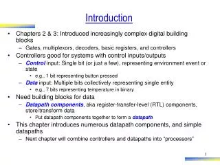
Introduction • Chapters 2 & 3: Introduced increasingly complex digital building blocks • Gates, multiplexors, decoders, basic registers, and controllers • Controllers good for systems with control inputs/outputs • Controlinput: Single bit (or just a few), representing environment event or state • e.g., 1 bit representing button pressed • Data input: Multiple bits collectively representing single entity • e.g., 7 bits representing temperature in binary • Need building blocks for data • Datapath components, aka register-transfer-level (RTL) components, store/transform data • Put datapath components together to form a datapath • This chapter introduces numerous datapath components, and simple datapaths • Next chapter will combine controllers and datapaths into “processors”
x b Combinational n1 logic n0 s1 s0 State register clk load I 3 I 2 I 1 I 0 4-bit register D D D D Q Q Q Q clk Q3 Q2 Q1 Q0 How extend to only load on certain cycles? Registers • Can store data, very common in datapaths • Basic register of Ch 3: Loaded every cycle • Useful for implementing FSM -- stores encoded state • For other uses, may want to load only on certain cycles a Basic register loads on every clock cycle
Register with Parallel Load • Add 2x1 mux to front of each flip-flop • Register’s load input selects mux input to pass • Either existing flip-flop value, or new value to load
1 0 0 0 0 0 0 1 1 1 1 0 1 Register Example using the Load Input: Weight Sampler • Scale has two displays • Present weight • Saved weight • Useful to compare present item with previous item • Use register to store weight • Pressing button causes present weight to be stored in register • Register contents always displayed as “Saved weight,” even when new present weight appears Scale Weight Sampler Save I 3 I 2 I 1 I 0 b a 3 pounds 2 pounds load clk Present weight Q3 Q2 Q1 Q0 3 pounds Saved weight
0 Register contents 0 1 1 0 after shift right shr_in A: 1001 (original) • Implementation: Connect flip-flop output to next flip-flop’s input Shift Register Register contents 1 1 0 1 • Shift right • Move each bit one position right • Shift in 0 to leftmost bit before shift right a Q: Do four right shifts on 1001, showing value after each shift a 0100 0010 0001 a 0000
Shift Register • To allow register to either shift or retain, use 2x1 muxes • shr: 0 means retain, 1 shift • shr_in: value to shift in • May be 0, or 1 • Note: Can easily design shift register that shifts left instead
Multifunction Registers • Many registers have multiple functions • Load, shift, clear (load all 0s) • And retain present value, of course • Easily designed using muxes • Just connect each mux input to achieve desired function Functions: s1 s0 Operation 0 0 Maintain present value 0 1 Parallel load 1 0 Shift right 1 1 (unused - let's load 0s)
Multifunction Registers s1 s0 Operation 0 0 Maintain present value 0 1 Parallel load 1 0 Shift right 1 1 Shift left
ld shr shl Operation 0 0 0 Maintain present value 0 0 1 Shift left 0 1 0 Shift right 0 1 1 Shift right – shr has priority over shl 1 0 0 Parallel load I 3 I 2 I 1 I 0 1 0 1 Parallel load – ld has priority shr_in 1 1 0 Parallel load – ld has priority 1 1 1 Parallel load – ld has priority I 3 I 2 I 1 I 0 shr_in ld s1 shl_in shl_in s0 shr Truth table for combinational circuit Q3 Q2 Q1 Q0 shl Inputs Outputs Note Operation shr shl s1 s0 ld Q3 Q2 Q1 Q0 0 0 Maintain value 0 0 0 1 1 Shift left 0 0 1 1 0 Shift right 0 1 0 c ombi- 1 0 Shift right 0 1 1 s1 = ld’*shr’*shl + ld’*shr*shl’ + ld’*shr*shl s0 = ld’*shr’*shl + ld n a tional 1 0 0 0 1 Parallel load ci r cuit 0 1 Parallel load 1 0 1 1 1 0 0 1 Parallel load 0 1 Parallel load 1 1 1 Multifunction Registers with Separate Control Inputs ? a a a
1 0 Shift right 0 1 0 0 1 X Shift right 1 0 Shift right 0 1 1 1 X X Parallel load 0 1 Parallel load 1 0 0 0 1 Parallel load 1 0 1 0 1 Parallel load 1 1 0 0 1 Parallel load 1 1 1 Register Operation Table • Register operations typically shown using compact version of table • X means same operation whether value is 0 or 1 • One X expands to two rows • Two Xs expand to four rows • Put highest priority control input on left to make reduced table simple Inputs Outputs No t e ld shr shl Ope r a tion Operation shr shl s1 s0 ld 0 0 Maintain value 0 0 0 0 0 0 M ai n tain v alue 1 1 Shift left 0 0 1 0 0 1 Shi f t le f t
Register Design Process • Can design register with desired operations using simple four-step process
s2 s1 s0 Operation 0 0 0 Maintain present value 0 0 1 Parallel load 0 1 0 Shift left 0 1 1 Synchronous clear 1 0 0 Synchronous set 1 0 1 Maintain present value 1 1 0 Maintain present value 1 1 1 Maintain present value In 1 0 from Qn-1 s2 7 6 5 4 3 2 1 0 s1 s0 D Q Qn Inputs Outputs s2 = clr’*set s1 = clr’*set’*ld’*shl + clr s0 = clr’*set’*ld + clr clr set ld shl s2 s1 s0 Operation 0 0 0 0 0 0 0 Maintain present value 0 0 0 1 0 1 0 Shift left 0 0 1 X 0 0 1 Parallel load 0 1 X X 1 0 0 Set to all 1s 1 X X X 0 1 1 Clear to all 0s Register Design Example • Desired register operations • Load, shift left, synchronous clear, synchronous set Step 1: Determine mux size 5 operations: above, plus maintain present value (don’t forget this one!) --> Use 8x1 mux a Step 2: Create mux operation table Step 3: Connect mux inputs Step 4: Map control lines a
Inputs Outputs s2 = clr’*set s1 = clr’*set’*ld’*shl + clr s0 = clr’*set’*ld + clr clr set ld shl s2 s1 s0 Operation 0 0 0 0 0 0 0 Maintain present value 0 0 0 1 0 1 0 Shift left 0 0 1 X 0 0 1 Parallel load 0 1 X X 1 0 0 Set to all 1s 1 X X X 0 1 1 Clear to all 0s Register Design Example I 3 I 2 I 1 I 0 I 3 I 2 I 1 I 0 shl s2 s1 shl_in combi- shl_in ld s0 national set circuit Q3 Q2 Q1 Q0 clr Q3 Q2 Q1 Q0 Step 4: Map control lines
1 0 0 0 0 1 0 1 0 0 1 0 1 1 1 0 1 0 1 0 0 1 0 1 1 1 0 1 1 1 0 0 0 1 1 1 1 0 1 1 0 0 1 1 1 0 1 0 1 1 1 1 1 1 1 0 Adders • Adds two N-bit binary numbers • 2-bit adder: adds two 2-bit numbers, outputs 3-bit result • e.g., 01 + 11 = 100 (1 + 3 = 4) • Can design using combinational design process of Ch 2, but doesn’t work well for reasonable-size N • Why not? Inputs Outputs a1 a0 b1 b0 c s1 s0 0 0 0 0 0 0 0 0 0 0 1 0 0 1 0 0 1 0 0 1 0 0 0 1 1 0 1 1 0 1 0 0 0 0 1 0 1 0 1 0 1 0 0 1 1 0 0 1 1 0 1 1 1 1 0 0
Inputs Outputs a1 a0 b1 b0 c s1 s0 0 0 0 0 0 0 0 0 0 0 1 0 0 1 0 0 1 0 0 1 0 0 0 1 1 0 1 1 0 1 0 0 0 0 1 0 1 0 1 0 1 0 0 1 1 0 0 1 1 0 1 1 1 1 0 0 1 0 0 0 0 1 0 10000 1 0 0 1 0 1 1 8000 1 0 1 0 1 0 0 6000 1 0 1 1 1 0 1 Transistors 1 1 0 0 0 1 1 4000 1 1 0 1 1 0 0 2000 1 1 1 0 1 0 1 1 1 1 1 1 0 1 0 1 2 3 4 5 6 7 8 N Why Adders Aren’t Built Using Standard Combinational Design Process • Truth table too big • 2-bit adder’s truth table shown • Has 2(2+2) = 16 rows • 8-bit adder: 2(8+8) = 65,536 rows • 16-bit adder: 2(16+16) = ~4 billion rows • 32-bit adder: ... • Big truth table with numerous 1s/0s yields big logic • Plot shows number of transistors for N-bit adders, using state-of-the-art automated combinational design tool Q: Predict number of transistors for 16-bit adder A: 1000 transistors for N=5, doubles for each increase of N. So transistors = 1000*2(N-5). Thus, for N=16, transistors = 1000*2(16-5) = 1000*2048 = 2,048,000. Way too many! a
0 1 1 1 1 1 1 1 1 1 1 1 + 0 1 1 0 + 0 1 1 0 1 0 A: 1 1 1 1 1 1 1 1 B: + 0 1 1 0 + 0 1 1 0 1 0 1 1 0 1 1 0 1 0 1 Alternative Method to Design an Adder: Imitate Adding by Hand • Alternative adder design: mimic how people do addition by hand • One column at a time • Compute sum, add carry to next column a
0 1 0 1 0 1 1 1 0 1 1 1 A: 1 + B: 0 1 1 0 b a ci b a ci b a ci b a c o s c o s c o s c o s 1 0 1 0 1 SUM Alternative Method to Design an Adder: Imitate Adding by Hand • Create component for each column • Adds that column’s bits, generates sum and carry bits 1 1 A: 1 1 1 1 B: + 0 1 1 0 a Half-adder Full-adders
1 1 0 a b I nputs O utputs 1 1 1 A: 1 a b a b c o s + 0 0 0 0 B: 0 1 1 0 0 1 0 1 c o s 1 0 0 1 co = ab s = a’b + ab’ (same as s = a xor b) a b a ci b a ci b a ci b 1 1 1 0 c o s c o s c o s c o s c o s 1 0 1 0 1 SUM Half-adder Half-Adder • Half-adder: Adds 2 bits, generates sum and carry • Design using combinational design process from Ch 2 Step 1: Capture the function Step 2: Convert to equations Step 3: Create the circuit
1 1 0 I nputs O utputs a b ci c o s 0 0 0 0 0 1 1 1 A: 1 Step 1: Capture the function 0 0 1 0 1 Step 3: Create the circuit Step 2: Convert to equations 0 1 0 0 1 + B: 0 1 1 0 0 1 1 1 0 co = a’bc + ab’c + abc’ + abc co = a’bc +abc +ab’c +abc +abc’ +abc co = (a’+a)bc + (b’+b)ac + (c’+c)ab co = bc + ac + ab s = a’b’c + a’bc’ + ab’c’ + abc s = a’(b’c + bc’) + a(b’c’ + bc) s = a’(b xor c)’ + a(b xor c) s = a xor b xor c a b ci 1 0 0 0 1 a b a ci b a ci b a ci b 1 0 1 1 0 c o s c o s c o s c o s 1 1 0 1 0 1 1 1 1 1 1 0 1 0 1 SUM Full adder s c o Full-Adder • Full-adder: Adds 3 bits, generates sum and carry • Design using combinational design process from Ch 2
a3 b3 a2 b2 a1 b1 a0 b0 a b ci a b ci a b ci a b a3 a2 a1 a0 b3 b2 b1 b0 F A F A F A HA 4-bit adder c o s c o s c o s c o s c o s3 s2 s1 s0 c o s3 s2 s1 s0 ( a ) ( b ) Carry-Ripple Adder • Using half-adder and full-adders, we can build adder that adds like we would by hand • Called a carry-ripple adder • 4-bit adder shown: Adds two 4-bit numbers, generates 5-bit output • 5-bit output can be considered 4-bit “sum” plus 1-bit “carry out” • Can easily build any size adder


