
1993
E N D
Presentation Transcript
1997 1993 1997
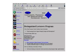
Paul Franzon Prof. Paul D. Franzon is currently a Professor at North Carolina State University. He earned his PhD from University of Adelaide, Australia in 1988. He has also worked at AT&T Bell Laboratories, DSTO Australia, Australia Telecom, Communica Ltd., and LightSoin Pty., Ltd. The latter two companies he cofounded. His current interests center on the technology and design of complex systems incorporating VLSI, MEMS, advanced packaging, optoelectronics, and nanotechnology. In 1993 he received an NSF Young Investigators Award and in 2001 was elected to the NCSU Academy of Outstanding Teachers. He is a member of theCPMT, CS, SSC, COMSOC, and CAS IEEE societies and of ACM. He has consulted at HP, SUN, Bell Northern Research, Cadence, Mentor Graphics, Ericsson. He has published over 80 papers, co-authored three books: Verilog Styles for Synthesis of Digital Systems, Multichip Modules: Basics and Alternatives, High Performance Design Automation for Multichip Modulesand Packages, many book chapters, invited presentations at Texas Instruments, DAC, Ford Microelectronics, IBM, GIT, IMAPS, SRC, Intel, DEC, SUN, received $9,000,000 research funding from NSF, SRC, ARPA, Sematech, MCNC, Motorola, DARPA. He has chaired IEEE MCM conference, TPC member of many other conferences, Associate Editor of IEEE Transactions on Advanced Packaging. Talk Abstract On-Chip Inductance On-chip parasitic and designed inductors greatly complicate IC design, modeling and measurement. This talk is a mix of a tutorial about on-chip inductance issues and a description of on-going work in new measurement techniques. Topics covered include on-chip signal integrity, the effects that parasitic inductance has on timing and noise, control approaches, design and measurement of on-chip spiral inductors and transformers, and S-parameter measurement of parasitic inductance.
Luc Martens Prof. Luc Martens received the M.Sc. degree in electrical engineering from Ghent University in July 1986. From September 1986 to December 1990 he was a research assistant at the Department of Information Technology (INTEC) of the same university. In December 1990 he obtained the Ph. D. degree from Ghent University. Since January 1991, he is a member of the permanent staff of the Interuniversity MicroElectronics Centre (IMEC) and is responsible for the research on characterization of packaging technologies with respect to high-frequency and EMC behavior at INTEC. Since April 1993 he is Professor at Ghent University. He is author of many publications in international conferences and journals. He has given numerous conference tutorials and in 1998, he has written the book High-frequency Characterization of Electronic Packaging (Kluwer Academic Publishers, ISBN 0-7923-8307-9). He is a member of the CPMT Society. Talk Abstract High-Frequency Measurement Techniques for Characterization of Electronic Packaging More and more the high-frequency or high-speed behavior of electronic packaging can not be neglected anymore in the system behavior. Experimental testing is a way to obtain the high-frequency characteristics. In this talk we will explain the basic and advanced principles of high-frequency measurements applied to electronic packaging. Especially problems related to the high-frequency characterization will be treated. Practical solutions will be proposed and illustrated with up-to-date examples. At the end of the talk, the participant should be able to design or select the best test fixture and measuring instrument for his or her application and to perform accurate high-frequency measurements. It will also be clear that circuit-modeling starting from the measurements is an essential part of the characterization process. The discussion of advantages and drawbacks of various measurement-based modeling algorithms will enable the participant to select the appropriate method.
George Katopis George Katopis is an IBM Distinguished Engineer and IEEE Fellow. In his current job assignment he is responsible for the package architecture and technology of the high end eServers for the IBM Corp. . George's background is in electrical engineering where he holds an MS in Electrical Engineering and Computer Science from Columbia University in the city of New York ( 1972) and an MPh in Engineering Science from the same University (1980). His areas of specialization is signal integrity design and algorithms, and electronic noise characterization and containment. He is the author of over 60 papers in the field of his specialization and was a lecturer in the distinguished lecturer series at several US Universities. He has authored and co-authored chapters in 5 engineering books and holds several patents in noise containment techniques. George has a large teaching experience in the US ( Fairleigh Dickinson adjunct professor 1973-1974, lecturer of many internal IBM courses on electrical design of packaging structures), and Europe ( CEI -Elsevier lecturer from 1989-1993). He is an SRC industrial mentor to the University of Arizona and Cornell University and chair for two years for the EPEP conference. He is member of the CPMT society. Talk Abstract Third Generation Signal Integrity Tools and Issues There exist two types of Signal integrity tool sets. One for the high level design of high performance packaging structures, and one for the verification of a package design after the interconnection wiring has been completed based on the rules and directions developed during the high level design. Not only the components of these tool sets are different, but also, even when the components of these tool sets are similar, their attributes are very different because of the different objectives that such components are required to fulfill. In this talk we will consider the tools used for the verification of the design of a package structure after its physical wiring has been completed. As we will show the ability to develop such tools presupposes the availability of adequate high level design signal integrity tools. This type of signal integrity tools includes accurate electrical parameter extractors for large physical structures, and accurate circuit analysis programs. It is to be noted that for this category of tools the main objective is their accuracy and ability to handle large physical structures, while their execution time is not as important for reasons that will become clear in the following. To the contrary for the verification tools the opposite is true. The development of both types of tools has started in IBM a long time ago, because of the needs of the mainframe computers that IBM has been provided to the market from the beginning of the computer age. Even the early versions of these systems required high frequency interconnections to support SMP servers ( Symmetric Multiprocessing ) that in turn required very large volumetric densities of the processor chips.
These requirements resulted in the use of Multi Chip Modules (or MCM) namely, ceramic structures carrying large numbers of the Silicon chips (either bipolar in the decade of 70s and 80s, or CMOS in the 90s), and a large number of interconnections ranging from 5000 to 18000. In addition, the design of such complicated systems required the involvement of different skills from different engineering areas, and hence the need of comprehensive hand shakes for the progression of the package design from one phase to the next. Clearly, one of the most important phases is the delivery of the paper design of an MCM for its implementation to manufactured product. This is even more important for the ceramic MCM technology due to its long manufacturing TAT ( Turn Around Time). Therefore, the first generation of package design verification tools was developed in IBM in the 80’s, in order to make sure that single pass design of MCMs could be achieved. The first generation of these tools was reflecting the technology needs and requirements but in addition, it established a set of attributes that such tools should have that transcends their particular application. In this presentation we shall describe these attributes that define the accuracy and execution time limitations, as well as the limitations that these tools had with respect to the interconnection topology considered. As the CMOS technology became the pervasive technology for all computing systems, and facilitated the significant increase of the interconnection speed and number of system components within one box, the needs of the mainframes in yesteryears became very similar to the needs for the field replaceable units of the current products. In addition, the continuously increasing speed of delivering products in the market place generated similar requirements for the package design verification tools as the long manufacturing TAT have done for the early MCM designs. Hence, the second generation of package design verification tools emerged that have the same attributes as the first generation verification tools, but they require techniques that minimize their development time, while increase their generality in analyzing interconnection topologies. The basic components of these tools will be discussed, their affinity to the first generation predecessors will be highlighted, and their limitation or tradeoffs will be identified. Based on this brief history in time for the package design verification tools, I will discuss my vision for the third generation of package verification tools and the impacts that the recent I/O developments will have on them. I shall show that even though the basic tool attributes remain the same their implementation need to be flexible to accommodate the new design criteria that emanate from the trend to asynchronous communications that will dominate the interconnection in the future server systems.