Antireflex coatings
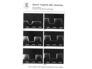
Antireflex coatings. Impact of standing waves on the developed resist. Resist was exposed both to the light source and to reflected beams from resist/sample interfaces. Problem solved after coating the film with an anti-reflex material (e.g. oxinitride) before exposure.

Antireflex coatings
E N D
Presentation Transcript
Antireflex coatings Impact of standing waves on the developed resist Resist was exposed both to the light source and to reflected beams from resist/sample interfaces Problem solved after coating the film with an anti-reflex material (e.g. oxinitride) before exposure Antireflex coating ARC @ INESC: 150, 400Å TiWN2
Next generation lithography • - vacuum environment • - direct write systems (software masks) • slow writting over large areas • very high system cost - Air environment - Complex mask fabrication ($4k-$12k) - Resists have low sensivity - High cost X-ray sources
X-ray lithography • Advantages: • No vacuum environment required (no charged particles involved) • Very small wavelength (< 14Å) - can produce 0.15 µm features • High reproducibility (exposure independent of substrate type, surface reflections) • Disadvantages: • No optics involved – limited to 1:1 shadow printing (no image reduction is possible) • Very expensive and complex mask fabrication (~10 days, cost is $4k-$12k) • Low sensivity of the resists • High cost of sufficiently bright X-ray sources • (e.g. Synchrotron)
E-beam lithography 10-100 keV electron beam • Advantages: • vacuum environment required (charged particles involved) • Direct write system (software mask) • the smaller the beam sizes, the better the resolution • can produce down to 0.01mm features • low defect densities • At 30 keV, electrons travel >14 mm deep into a resist layer • Disadvantages: • Very expensive system • Slow writting Leica EBL-100, shown here with a 100 kV LaB6 electron source and a conventional SEM stage. The system is also available with a TFE source and laser-controlled stage. (Courtesy of Leica Lithography Systems Ltd.) COSTS ~$1M, for 2 inch areas maximum.
Ion Beam lithography • Advantages: • Computer-controlled beam • No mask is needed • Can produce sub-1 µm features • Resists are more sensitive than electron beam resists • Diffraction effects are minimized • Less backscattering occurs • Higher resolution • Ion beam can detect surface features for very accurate registration • Disadvantages: • Reliable ion sources needed • Swelling occurs when developing negative ion beam resists, limiting resolution • Expensive as compared to light lithography systems • Slower as compared to light lithography systems • Tri-level processing required
ΔE ~ 6 eV (75KeV) Paul Scherrer Institute Electrom Beam Lithography System Multi-Cusp Ion Source http://lmn.web.psi.ch Ion Beam Source Ion Optics ΔE ~ 0.5 eV (75KeV) Co-axial Ion Source Vacuum Chamber Ion energies : 20 eV - 200 KeV Beam Current : up to 500 A/cm2 Ion Specimens : H, He,Ar, Hf, Ga, Si, Au, Co, Pr, P+, BF2+, etc…
Ion Beam Cannon Focused Ion Beam Lithography (FIBS) Scanning Beam Exposure System Feature size is limited by spot size Allows the exposure of very complex patterns in only one lithography step Can take up to 6 orders of magnitude longer than mask projection technology, depending on sample size ⇨ Not suitable for Industrial Purposes
Bibliography • VLSI Technology, S.M.Sze, McGraw-Hill International Editions • Nanoelectronics and information technology – Advanced Electronic Materials and • Novel Devices, Rainer Waser (Ed.), Wiley-VCH (2003) • Microsystems: mechanical, chemical, optical, S.D.Sentura, M.A.Schmidt and J.Harrison, MIT press • Fundamentals of Microfabrication – The science of miniaturization, Marc J.Madou, CRC press (2002) • Spin Electronics - Chap.16, M.Ziese and M.J.Thornton (Ed.), Lecture Notes in Physics, Springer-Verlag • http://www.cnf.cornell.edu/spiebook/toc.htm • http://semiconductorglossary.com/default.asp?searchterm=lithography

