Download
1 / 20
210 likes | 386 Vues
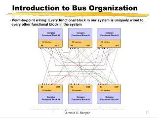
Introduction to Bus Organization. Point-to-point wiring: Every functional block in our system is uniquely wired to every other functional block in the system. Introduction to Bus Organization. Complex Functional Block #1. IN. CONTROL. OUT. CONTROL. I/O Interface.

E N D
Introduction to Bus Organization • Point-to-point wiring: Every functional block in our system is uniquely wired to • every other functional block in the system Hardware Computer Organization for the Software Professional Arnold S. Berger
Introduction to Bus Organization Complex Functional Block #1 IN CONTROL OUT CONTROL I/O Interface INPUT DECISION LOGIC OUTPUT DECISION LOGIC In from #2 In from #3 In from #4 In from #5 In from #6 Out to #2 Out to #3 Out to #4 Out to #5 Out to #6 Single bit inputs from other blocks Single bit outputs to other blocks Hardware Computer Organization for the Software Professional Arnold S. Berger
Bus organization How do we manage the flow of information? Hardware Computer Organization for the Software Professional Arnold S. Berger
Bus organization • Busses were invented in order to simplify the organization and flow of data within computer systems • Busses allow many devices to connect to the the same data path • Allow for efficient exchange of data between devices • Question: How do I connect outputs together and not get a short circuit? BUS 1 (5V) 1 0 (0V) 1 AND Gate 1 AND Gate 2 1 0 Short circuit ( bus contention) Actual result will be an indeterminate logic level Hardware Computer Organization for the Software Professional Arnold S. Berger
Bus organization(2) • Answer: All logic devices that connect to a bus are actually divided into two parts: Logic functional block and bus interface unit Bus Interface Input Logic Function • Bus control • Close the switch > output connected • Open the switch > output disconnected BUS Hardware Computer Organization for the Software Professional Arnold S. Berger
8-bit Data Bus DB0 DB1 DB2 DB3 DB4 DB5 DB6 DB7 Connection Symbol Bus Interface CE Actual Logic inputs DB7 DB6 DB5 DB4 DB3 DB2 DB1 DB0 Hardware Computer Organization for the Software Professional Arnold S. Berger
Tristate bus organization D0 D0 D0 D0 32-bit register 32-bit register 32-bit register 32-bit register D31 D31 D31 D31 CS2 CS1 CS3 • With a tristated bus, outputs can be connected directly to the bus, but the chip select signals must be controlled through appropriate addressing • Suggested exercise: Derive the Truth Table for a 2:4 decoder Data Bus D0..D31 A0 A1 CS0 2:4 Address Decoder Hardware Computer Organization for the Software Professional Arnold S. Berger
Algorithmic State Machine Revisited DATA BUS Temporary Register Register A Register B Arithmetic and logic unit (ALU) clk_A oe_A clk_B oe_B clk_t ALU_0 ALU_1 ALU_2 ALU Output Register C Microsequence Controller oe_OUT clk_OUT System Clock in Hardware Computer Organization for the Software Professional Arnold S. Berger
Why do we need an ASM? • Bus organization simplifies data routing • ASM provides mechanism for sequencing multiple operands on the internal busses of the processor • Question: What might the state transition table for the addition operation look like for the operation <reg A> + <reg B> <reg A>? ALU_1 ALU_2 oe_A oe_B oe_OUT ALU_1 ALU_2 clk_A clk_A ALU_0 clk_OUT oe_A oe_B clk_T clk_B ALU_0 clk_OUT oe_OUT clock clk_B clk_T Hardware Computer Organization for the Software Professional Arnold S. Berger
A “D” flip-flop memory cell A single bit memory cell DATA I/O Q D W CLK OE Flip-flop core Without S,R and Q Tri-state buffer Hardware Computer Organization for the Software Professional Arnold S. Berger
Memory organization Q Q Q Q Q Q Q Q Q Q Q Q Q Q Q Q D D D D D D D D D D D D D D D D CLK CLK CLK CLK CLK CLK CLK CLK CLK CLK CLK CLK CLK CLK CLK CLK OE OE OE OE OE OE OE OE OE OE OE OE OE OE OE OE DB0 DB1 DB2 DB3 A0 A1 (W0)D0..D3 (OE0)D0..D3 CS Memory decoding logic (W1)D0..D3 R / W (OE1)D0..D3 (W2)D0..D3 (OE2)D0..D3 (W3)D0..D3 (OE3)D0..D3 Hardware Computer Organization for the Software Professional Arnold S. Berger
Paging 64K Page 0 64K Page 1 64K Page E 64K Page F • Can create larger memory arrays but is difficult to manage across page boundaries • Generally not supported by commercial compilers • Useful for programs designed with overlays • Similar to how virtual memory is handled by operating systems • Example: Suppose that you have a processor with a 20-bit (220) addressing range and you are using memories with 64K addressing A15-A0 uP CS CS CS CS 1110 1111 0000 0001 A19-A16 Page select (4 to 16 decoder) Hardware Computer Organization for the Software Professional Arnold S. Berger
Page size options • Paging is the fundamental method of organizing memory in computer systems • In the previous example, we organized a 1 Mbyte memory space (20-bit ) as 16, 64Kbyte pages • We could have represented the address in many other ways: Page address Offset address bits Page address bits Page offset 0 to 1,048,575 NONE Linear address A0 to A19 NONE A19 0 to 524,287 A0 to A18 0 to 1 A19-A18 0 to 262,143 A0 to A17 0 to 3 A19-A17 A0 to A16 0 to 7 0 to 131,071 A19-A16 A0 to A15 Our example 0 to 65,535 0 to 15 A19-A15 0 to 32,767 A0 to A14 0 to 31 A19-A14 0 to 16,383 A0 to A13 0 to 63 Hardware Computer Organization for the Software Professional Arnold S. Berger
Decoding the memory space W W W W A0 A0 A0 A0 D0 D0 D0 D0 A1 A1 A1 A1 D1 D1 D1 D1 A2 A2 A2 A2 A3 A3 A3 A3 A4 A4 A4 A4 D2 D2 D2 D2 A5 A5 A5 A5 A6 A6 A6 A6 D3 D3 D3 D3 A7 A7 A7 A7 A8 A8 A8 A8 D4 D4 D4 D4 A9 A9 A9 A9 A10 A10 A10 A10 D5 D5 D5 D5 A11 A11 A11 A11 A12 A12 A12 A12 D6 D6 D6 D6 A13 A13 A13 A13 A14 A14 A14 A14 D7 D7 D7 D7 CE CE CE CE OE OE OE OE Address Bus: A0..A14 • Design the SRAM memory system using 256-Kbit ( 32K x 8 ) SRAM chips To uP W OE A15..A23 ADDR VAL ADDRESS DECODE LOGIC RD CE0 WR CE1 To uP Data Bus: D0..D15 Hardware Computer Organization for the Software Professional Arnold S. Berger
Expanding memory by width W W A0 A0 D0 D0 A1 A1 D1 D1 A2 A2 A3 A3 A4 A4 D2 D2 A5 A5 A6 A6 D3 D3 A7 A7 A8 A8 D4 D4 A9 A9 A10 A10 D5 D5 A11 A11 A12 A12 D6 D6 A13 A13 A14 A14 D7 D7 CE CE OE OE D0 D1 D2 D3 D4 D5 D6 D7 D8 D9 D10 D11 D12 D13 D14 D15 16-bit data bus, D0..D15 Hardware Computer Organization for the Software Professional Arnold S. Berger
Memory decoding • Suppose that our page size is 32K (214 ) • When A15 through A23 = 1 AND the processor asserts that the address is valid, then the highest 32K page of memory will be enabled Hardware Computer Organization for the Software Professional Arnold S. Berger
Notes about DRAM memory • Reading and writing to a memory location causes the capacitor to be recharged ( refreshed ) • But how do you read or write to all the memory cells in enough time ( ~10 milliseconds ) in order to guarantee that no data is lost? • Solution: You “sort of read” a group of cells at a time 13 Column Address Lines CA0..CA12 (0,8191) (0,1) (0,0) EXAMPLE: A 64-Mbit DRAM (1,0) 13 Row Address Lines RA0..RA12 (8191,0) (8191,8191) Hardware Computer Organization for the Software Professional Arnold S. Berger
Microprocessor component systems • Three major busses of a microprocessor • Address bus: Unidirectional • Data bus: Bidirectional • Status bus: Heterogeneous, additional control and housekeeping signals Address Bus: Out to Memory 16 Mbyte address space or 8 M words A1..A23 D0..D15 Status Bus Data Bus: Out to Memory Input from Memory MC68000 • RESET • INTERRUPT • BUS REQUEST • BUS ACKNOWLEDGE • CLOCK IN/OUT • READ/WRITE • BYTE WRITE SELECTORS Hardware Computer Organization for the Software Professional Arnold S. Berger
Microprocessor timing • These are the gory details of a typical bus cycle Memory Read Cycle Memory Write Cycle T1 T2 T3 T1 T2 T3 CLK Address Valid Address Valid ADDRESS A0..AN ADDR VAL RD WR Data Valid Data Valid DATA D0..DN WAIT Hardware Computer Organization for the Software Professional Arnold S. Berger
Direct Memory Access (2) • In its simplest form, there is a handshake process between the processor and the peripheral device • Peripheral device requests control of the bus from the processor • BUS REQUEST (BUSREQ) • When processor completes present instruction cycle and no higher level interrupts are pending, it sends out a BUS GRANT (BUSGRA), giving the requesting device permission to begin its own memory cycles • Processor then idles until BUSREQ signal goes away Address, Data and Status Busses BUSREQ uP MEMORY ARRAY PERIPHERAL DEVICE BUSGRA Hardware Computer Organization for the Software Professional Arnold S. Berger