Enhancing Gas Sensing in Zinc Oxide Field-Effect Sensors with Gold Nanoparticles
Gas sensors based on zinc oxide were enhanced by incorporating Au nanoparticles, resulting in improved sensitivity to CO gas. XPS analysis confirmed the presence of metallic gold nanoclusters on the ZnO surface. Sensitivity and response time were significantly enhanced in ZnO/Au devices compared to pure ZnO sensors. Further research is needed to understand the chemical mechanisms involved and explore the effect on other gases. The study, conducted at leading research institutes, offers valuable insights into optimizing gas sensor performance.

Enhancing Gas Sensing in Zinc Oxide Field-Effect Sensors with Gold Nanoparticles
E N D
Presentation Transcript
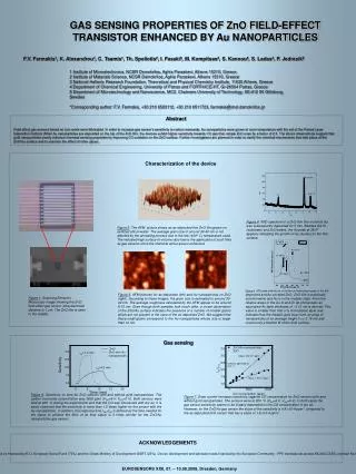
Abstract Field effect gas sensors based on zinc oxide were fabricated. In order to increase gas sensor’s sensitivity to carbon monoxide, Au nanoparticles were grown at room temperature with the aid of the Pulsed Laser Deposition method. When Au nanoparticles are deposited on the top of the ZnO film, the devices exhibit higher sensitivity towards CO gas than simple ZnO ones by a factor of 2.5. The above observations suggest that gold nanoparticles clearly enhance chemical sensing properties by improving CO oxidation on the ZnO surface. Further investigations are planned in order to clarify the chemical mechanisms that take place at the ZnO/Au surface and to examine the effect of other gases. Figure 5. XPS peak intensity as a function of the binding energy for the as-deposited and Au-covered ZnO.ZnO film is practically stoichiometric and Au is in the metallic state. From the relative areas of the Au 4f and Zn 3p photopeaks an equivalent Au layer thickness of ~0.16 nm is derived. This value is smaller than that of a monoatomic layer and indicates that the metallic gold must form an array of nanoparticles of an average height h >> 0.16 nm and covers only a fraction Θ of the ZnO surface. Figure 3. AFM pictures for as-deposited (left) and Au nanoparticles on ZnO (right). According to these images, the grain size is estimated to around 30-40 nm. The average roughness calculated by the AFM appear to be around 9-10 nm. Even though both samples look much alike, a closer observation of the ZnO/Au surface indicates the presence of a number of smaller grains which are not present in the case of the as-deposited ZnO. We suggest that these small grains correspond to the Au nanoparticles whose size is larger than 10 nm. Figure 6. Sensitivity vs time for ZnO sensors with and without gold nanoparticles. The carbon monoxide concentration was 3800 ppm (VDS=6 V, VGS=0 V). Both sensors were held at 200 C during the experiments and that the CO was introduced with dry air. It is easily observed that the sensitivity is more than 1.5 times higher for the sensor with the Au nanoparticles. In addition, the response time τ90(τ90 is defined as the time needed for the signal to achieve the 90% of its final value) is 3 times shorter for the ZnO/Au nanoparticles gas sensor. Figure 7. Drain current increase (sensitivity) against COconcentration for ZnO sensors with and without gold nanoparticles. The sensors were at 200 C (VDS=6 V, VGS=0 V). In both cases the gas sensor sensitivity seems to be linearly depended on the CO concentration in dry air. However, for the ZnO/Au gas sensor the slope of the sensitivity is 4.8 x10⁻⁴ ppm-1 compared to the as-deposited ZnO sensor that has a slope of 1.9 x10⁻⁴ ppm-1. GAS SENSING PROPERTIES OF ZnO FIELD-EFFECT TRANSISTOR ENHANCED BY Au NANOPARTICLES F.V. Farmakis1, K. Alexandrou1, C. Tsamis1, Th. Speliotis2, I. Fasaki3, M. Kompitsas3, S. Kennou4, S. Ladas4, P. Jedrasik5 1 Institute of Microelectronics, NCSR Demokritos, Aghia Paraskevi, Athens 15310, Greece 2 Institute of Materials Science, NCSR Demokritos, Aghia Paraskevi, Athens 15310, Greece 3 National Hellenic Research Foundation, Theoretical and Physical Chemistry Institute, 11635 Athens, Greece 4Department of Chemical Engineering, University of Patras and FORTH/ICE-HT, Gr-26504 Patras, Greece 5 Department of Microtechnology and Nanoscience, MC2, Chalmers University of Technology, SE-412 96 Göteborg, Sweden *Corresponding author: F.V. Farmakis, +30 210 6503112, +30 210 6511723, farmakis@imel.demokritos.gr . Characterization of the device Figure 4. XRD spectrum of a ZnO thin film on which Au was subsequently deposited for 5 min. Besides the Si (substrate) and ZnO peaks, the Au peak at 38.5O appears indicating the growth of Au clusters on the film surface. Figure 2. The AFM picture shows an as-deposited thin ZnO film grown on oxidized silicon wafer. The average grain size of around 30-40 nm is not affected by the annealing process due to the low (400O C) temperature used. The indicated high surface-to-volume ratio favors the application of such films as gas sensors since the chemical active area is enhanced. Figure 1. Scanning Emission Microscopy image showing the ZnO field-effect gas sensor. Intra-electrode distance is 1 μm. The ZnO film is seen in the middle. Gas sensing ACKNOWLEDGEMENTS This research project is co-financed by E.U.-European Social Fund (75%) and the Greek Ministry of Development-GSRT (25%). Device development and fabrication was financed by the European Community - FP6 translational access MC2ACCESS, contract No 026029. EUROSENSORS XXII, 07. – 10.09.2008, Dresden, Germany