Download
1 / 4
40 likes | 61 Vues
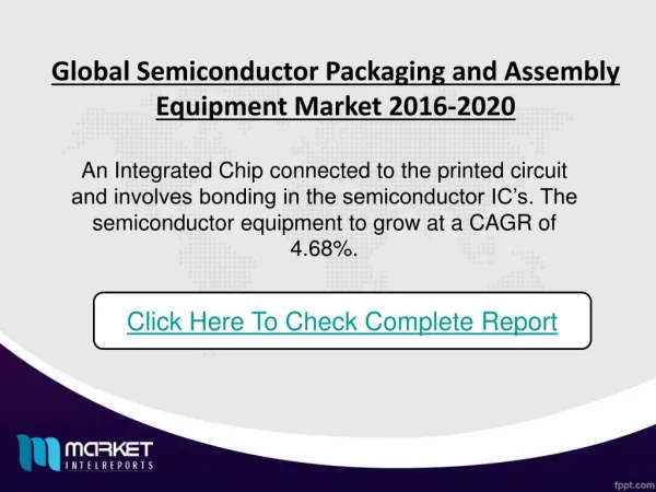
The Global Semiconductor Packaging and Assembly Equipment Market is classified on the basis of product type, end users and geography. The factors that propel the growth of the Semiconductor Packaging and Assembly Equipment Market include increasing application of semiconductor ICs in the IoT, increasing demand for polymer adhesive wafer bonding equipment, growing miniaturization of electronic devices, growing implementation of advanced packaging techniques and rising application of semiconductor ICs in IoT. On contrary, there are certain factors that may hamper the growth of the market such as need for huge investments. In addition, one of the major challenges for the growth of this market is unstable rates of foreign exchange.

E N D
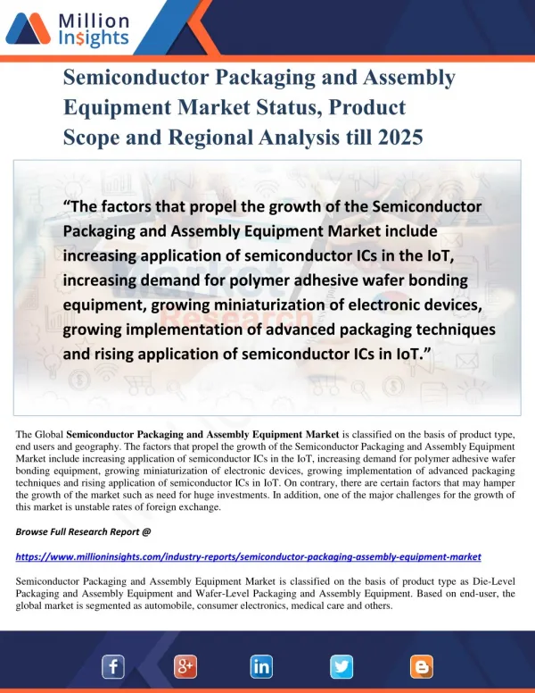
Semiconductor Packaging and Assembly Equipment Market Status, Product Scope and Regional Analysis till 2025 “The factors that propel the growth of the Semiconductor Packaging and Assembly Equipment Market include increasing application of semiconductor ICs in the IoT, increasing demand for polymer adhesive wafer bonding equipment, growing miniaturization of electronic devices, growing implementation of advanced packaging techniques and rising application of semiconductor ICs in IoT.” The Global Semiconductor Packaging and Assembly Equipment Market is classified on the basis of product type, end users and geography. The factors that propel the growth of the Semiconductor Packaging and Assembly Equipment Market include increasing application of semiconductor ICs in the IoT, increasing demand for polymer adhesive wafer bonding equipment, growing miniaturization of electronic devices, growing implementation of advanced packaging techniques and rising application of semiconductor ICs in IoT. On contrary, there are certain factors that may hamper the growth of the market such as need for huge investments. In addition, one of the major challenges for the growth of this market is unstable rates of foreign exchange. Browse Full Research Report @ https://www.millioninsights.com/industry-reports/semiconductor-packaging-assembly-equipment-market Semiconductor Packaging and Assembly Equipment Market is classified on the basis of product type as Die-Level Packaging and Assembly Equipment and Wafer-Level Packaging and Assembly Equipment. Based on end-user, the global market is segmented as automobile, consumer electronics, medical care and others.
Based on geographic segmentation, the global market spans North America, Latin America, Western Europe, Eastern Europe, Asia Pacific, Japan and Middle East and Africa. The North American region consists of the U.S., and Canada. Latin America region consists of Mexico and Brazil. The Western European region consists of Germany, Italy, France, England and Spain. The Eastern European region consists of Poland and Russia. Asia Pacific region consists of China, India, ASEAN, Australia & New Zealand. The Middle East and Africa region consists of GCC, South Africa and North Africa. Some of the key players that fuel the growth of the Semiconductor Packaging and Assembly Equipment Market include Applied Materials, ASMPT, DISCO, EVG, Kulicke and Soffa Industries, TEL, and Tokyo Seimitsu. The other prominent players that are operating in the Semiconductor Packaging and Assembly Equipment Market include Rudolph Technologies, SEMES, Suss Microtec, Ultratech, Ulvac Technologies, and others. Get a Sample Copy of This Report @ https://www.millioninsights.com/industry-reports/semiconductor-packaging-assembly-equipment-market/request-sample Market Segment: Geographically, this report is segmented into several key Regions, with production, consumption, revenue (million USD), market share and growth rate of Semiconductor Packaging and Assembly Equipment in these regions, from 2013 to 2025 (forecast), covering • North America • Europe • China • Japan • Southeast Asia • India Global Semiconductor Packaging and Assembly Equipment market competition by top manufacturers, with production, price, revenue (value) and market share for each manufacturer; the top players including • Applied Materials • ASM Pacific Technology (ASMPT) • Disco • EV Group (EVG) • Kulicke and Soffa Industries
• Tokyo Electron Ltd. (TEL) • Tokyo Seimitsu • Rudolph Technologies • SEMES • Suss Microtec See More Reports of This Category by Million Insights @ https://www.millioninsights.com/industry/machinery-and-machine-parts On the basis of product, this report displays the production, revenue, price, market share and growth rate of each type, primarily split into • Die-level packaging and assembly equipment • Wafer-level packaging and assembly equipment On the basis of the end users/applications, this report focuses on the status and outlook for major applications/end users, consumption (sales), market share and growth rate for each application, including • Consumer Electronics • Automobile • Medical Care • Others Browse Full Research Report @ https://www.millioninsights.com/industry-reports/semiconductor-packaging-assembly-equipment-market
Get in touch At Million Insights, we work with the aim to reach the highest levels of customer satisfaction. Our representatives strive to understand diverse client requirements and cater to the same with the most innovative and functional solutions. Contact Person: Ryan Manuel Research Support Specialist, USA Email: ryan@millioninsights.com Global Headquarters Asia Pacific Million Insights Million Insights Felton Office Plaza 6265 Highway 9 Felton, California 95018, United States Office No. 302, 3rd Floor, Manikchand Galleria, Model Colony, Shivaji Nagar, Pune, MH, 411016 India Phone: 1-408-610-2300 Email: sales@millioninsights.com Phone: 91-20-65300184 Email: sales@millioninsights.com Visit Our Blog: www.millioninsights.blogspot.com