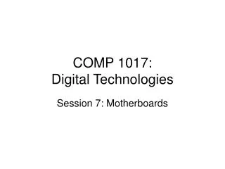
COMP 1321 Digital Infrastructure
250 likes | 377 Vues
This resource provides an in-depth explanation of the Fetch-Execute Cycle, a fundamental process within a CPU. It details how CPU instructions are executed sequentially, using examples from the Intel 8086 family. You'll learn about the role of registers, memory addresses, and how data is processed. The material also illustrates the CPU's speed and efficiency in processing instructions one at a time, along with key CPU types and their features. Explore how calculations and data handling occur within the CPU framework.

COMP 1321 Digital Infrastructure
E N D
Presentation Transcript
COMP 1321 Digital Infrastructure Richard Henson University of Worcester October2012
Week 3: The Fetch-Execute Cycle • Explain the instruction set of a typical CPU • Understand the sequential way a CPU works, using its instruction set • Understand how registers and memory addresses are used to process a CPU instruction and store the results
CPUs and the SAM • SAM designed to allow you to watch what happens when a CPU works • CPU very, very, very fast • Processes one instruction at a time • Instructions can require several cycles
What is “Processing”? • Usually calculations: • need data input • from register • from external memory • need to store output • from register • from external memory • Could also be a command without data
CPU types • Most frequently used: • Intel 8086 family • Motorola 68000 family • ARM (many mobile phones) • We’ll focus on Intel 8086 family • dates back to original IBM PC…
Registers • Tiny memory stores inside the CPU • usually containing one word of memory • Examples here show an 8-bit word (as used with original 8080 chip) • Typical registers: • general purpose data: AX, BX, CX, DX • specific use e.g. • program counter: instruction address in memory • stack pointer…
Data and Addressing • A general purpose register could contain • data • an address that points to data • Needs to be a way to distinguish between them • AX, 37 – move “37” into register • AX, [37] – move data contain in address 37 into register
8086 in practice • General Purpose registers 16-bit • Each gen register split into upper & lower byte lower byte upper byte AX AL AH BX BL BH CX CH CL DH DL DX
Fetch-Execute Cycle (Organization and Control) 1. Fetch instruction from memory 5. Write back results to registers ax <- ALU add ax , bx 4. Do any Memory Access 2. Decode the instruction and read any registers (Data cache) None needed ALU <- ax ALU <- bx 3. Do any ALU operations (execute units) ax + bx
0 1 2 3 4 Fetch-Exec : State 1 Instruction Fetch add ax , bx ax bx add AX BX 3 add ax,bx 3 1 8 7 1 9
0 1 2 3 4 Fetch-Exec : State 2 Decode, Register Operations add ax , bx ax bx add AX BX 3 add ax,bx 3 1 8 7 1 3 1 9
0 1 2 3 4 Fetch-Exec : State 3 ALU Operation add ax , bx ax bx add AX BX 3 add ax,bx 8 7 1 3 1 4 9
0 1 2 3 4 Fetch-Exec : State 4 Memory Access add ax , bx ax bx add AX BX 3 add ax,bx 8 7 1 3 1 4 9
0 1 2 3 4 Fetch-Exec : State 5 Register Write add ax , bx ax bx add BX 3 add ax,bx 4 8 7 1 3 1 4 9
Fetch-Execute Cycle (Organization and Control) 1. Fetch instruction from memory 5. Write back results to registers Data into ax mov ax , [1] 4. Do any Memory Access 2. Decode the instruction and read any registers Read memory at addr ‘1’ Read the ‘1’ 3. Do any ALU operations (execute units) Put ‘1’ into MAR
0 1 2 3 4 Fetch-Exec : State 1 Instruction Fetch mov ax , [1] mov ax 1 mov ax , [1] 3 8 7 1 9
0 1 2 3 4 Fetch-Exec : State 2 Decode, Register Operations mov ax , [1] mov ax 1 mov ax , [1] 3 8 7 1 9
0 1 2 3 4 Fetch-Exec : State 3 ALU Operation mov ax , [1] mov ax 1 mov ax , [1] 3 8 7 1 1 9
0 1 2 3 4 Fetch-Exec : State 4 Memory Access mov ax , [1] mov ax 1 mov ax , [1] 3 8 8 7 1 1 9
0 1 2 3 4 Fetch-Exec : State 5 Register Write mov ax , [1] mov ax 1 mov ax , [1] 3 8 8 8 7 1 1 9
Inside the 8088 address bus address adder External buses gen registers ALU
Pentium 1 2 • Fetch • Decode • ALU • Mem Ops • Reg Write 3 4 5
So THAT’S how it all works!now you try it on SAM2…Next week: a focus on writing programs and i/o