Download
1 / 23
230 likes | 362 Vues
This project, led by Anna Macchiolo at CiS and in collaboration with various ATLAS and CMS groups, focuses on enhancing planar pixel sensor technology for the SLHC. It aims to explore the application range for n-in-n and n-in-p sensor designs, optimizing wafer layouts and comparing performance metrics such as yield, reliability, and radiation hardness. Innovations include slim edges for increased active area, cost reductions, and advanced isolation techniques. This research supports future upgrades in pixel sensor technologies, ensuring efficiency and robustness in high radiation environments.

E N D
Planar Pixel Sensor Production at CiS Anna Macchiolo - MPP Munich • Project aimed to explore the possible range of application in fluence (hence detector radii) for planar pixels sensors at SLHC. • Wafer layouts for the n-in-n and n-in-p batches have been submitted to CiS • R&D areas to be covered by this project: • Comparison of performances between n- and p-bulk pixels: yeald, reliability, radiation hardness • Slim edges, increase of the fraction of active area • Cost reduction • Vertical integration
R&D for Planar Pixel Sensors for SLHC • Common RD50 production with the contribution of: • ATLAS groups participating in the Planar Pixel Sensor Project (coordinator C. Goessling, TU Dortmund), established in view of the Insertable B-Layer upgrade and SLHC • CMS pixel group at PSI • Parallel productions of n-on-p pixel sensors on 6” wafers within the ATLAS Planar Pixel Sensor Project : • HPK, organized by the KEK group • MICRON, organized by the Liverpool group • Planar technology is a natural baseline for pixel upgrades: • proven and reliable • recent data from the RD50 Collaboration indicate sufficient radiation hardness even at b-layer fluences • thanks to using industrial standard processes, cost effective production of large pixel sensor areas is achievable
Foreseen production parameters • Production with CiS (Erfurt, Germany) on 4” wafers • Parallel production of n-in-p and n-in-n wafers with several common test devices to achieve a full comparison between the two technologies • Inter-pixel isolation methods: homogenous p-spray and moderated p-spray for both batches
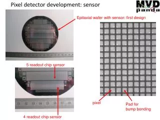
Wafer layout of the n-in-p batch • FE-I3 (present ATLAS ASIC) Single Chip Modules (SCM) with variations of the GR structure and isolation schemes • FE-I4: new ATLAS pixel ASIC (for IBL and SLHC outer layers): pitch 50x250 mm2, 22,6 x 19,2 mm². • CMS Module (16 chips) + 5 SCM same geometry as in the present CMS n-in-n sensors (design by T. Rohe). • 80 mm pitch strips: 4 sensors with the RD50 standard design (large inactive edge for cutting trials) and 2 with a MPP-HLL design (AC coupled).
Wafer layout of the n-in-n batch • 20 different SCM FE-I3 versions (see slides about slim edges). • Included the design of n-in-p SCM with GR on the front sidecomparison to real p-bulk after type conversion • FE-I4 4-chips Module: • Current ATLAS pixel guard ring design • Proposed sensor for the Insertable b-Layer (IBL): because of the length of the sensor it is possible to reach an inactive fraction of ~1.5% (without shingling) using the current guard ring design. • 2 samples of FE-I4 SCM • RD50 design strip detectors adapted to n-in-n technology. n-in-n design realized by the Dortmund group (T. Wittig)
ATLAS pixels: Isolation schemes (I) • Standard SCM dimensions , 1100 mm from cutting edge to guard rings • Moderated p-spray: standard isolation scheme between pixels adopted by the present n-in-n ATLAS and CMS sensors. • An opening in the nitride layer determines an increase of the boron implanted dose in the central region between the strips. Moderated p-spray 545 16 rings Moderated p-spray n+ n+ nitride opening p-spray Uniform p-spray
ATLAS pixels: Isolation schemes (II) Homogenous p-spray Moderated p-spray 545 16 rings 635 19 rings Homogenous p-spray Moderated p-spray • Implementation in the pixel design of the isolation scheme with homogenous p-spray : good performances observed in the pre-irradiation characterization of the MPP-HLL thin pixel production where this isolation method was implemented (see M. Beimforde’s talk, this workshop). • Effects of different p-spray implantation parameters simulated and tested with CiS p-type micro-strip detectors irradiated with X-rays: isolation holds after irradiation also for very low p-spray doses (~ 0.7x1012 cm-2) (M.Beimforde, 13th RD50 Workshop).
ATLAS p-type pixels: Guard Ring Design (I) • The guard-ring design used in the p-type CiS pixel submission is based on the one implemented in the MPI-HLL thin pixel production. Performances of these sensors in terms of Vbreak are extremely good. Still some possible improvements suggested by the pre-irradiation characterization of these devices. • Investigation of the breakdown location with PHEMOS:probe-station equipped with a CCD camera to detect hot spots in the sensor. • Structures with homogenous p-spray: breakdown in the GRs @ 425 V
ATLAS p-type pixels: Guard Ring Design (I) • The guard-ring design used in the p-type CiS pixel submission is based on the one implemented in the MPI-HLL thin pixel production. Performances of these sensors in terms of Vbreak are extremely good. Still some possible improvements suggested by the pre-irradiation characterization of these devices. • Investigation of the breakdown location with PHEMOS:probe-station equipped with a CCD camera to detect hot spots in the sensor. • Structures with moderated p-spray: breakdown in the GRs @ 585 V redesign of the 4th and 5th rings for the CiS production • The location of the hot spot in the bottom left corner is probably linked with the direction of the small misalignments among the different layers
ATLAS p-type pixels: Guard Ring Design (II) SOI hom. p-spray 1 1 2 2 3 3 4 4 SOI mod. p-spray CIS mod. p-spray 1 1 5 2 2 5 3 3 4 4 5 6 5 CiS design: Increase of the metal overhang on the inner side of the 4th and 5th rings both for the moderated and homogenous p-spray versions Thanks to Rainer Richter for discussions and suggestions Rings #1 and #2 in the CiS design are wider but with the same inter-distances and overhang structure as in the SOI ones CIS hom. p-spray
Area of R&D: Slim Edges for ATLAS SLHC Pixel Detector • Outer staves in the SLHC ATLAS pixel detector will probably be double-sided. In the inner layers of the pixel system (single-sided) it is strongly desired to avoid shingling: - deteriorates thermal performances - complicates stave design and add cost slim edges needed at least on two sides! Moderated p-spray Moderated p-spray 545 16 rings • Different methods explored to achieve a larger fraction of active area: - fewer guard rings (both n- and p-type) - instrument with pixels the area corresponding to the guard ring on the back-side (n-in-n only) - alternative dicing method with respect to sawing (laser and DRIE)
Slim Edges: reduced guard ring structures n-in-p • Design of slimmed guard-rings structures aided by simulation activities carried out by the ATLAS LAL-LAPNHE groups. • Both in the n-in-n and n-in-p designs the slimmed edge versions have been implemented mostly in the FE-I3 sensors more variations are possible due to the reduced size with respect to the FE-I4 sensors • Encouraging results from the MPP-HLL thin pixel production : p-type diodes with a reduced set of guard rings (10 guard rings, homogenous p-spray) yield the same Vbreak (~ 400-500 V depending on p-spray dose) as those with the standard guard-ring structure. Moderated p-spray Moderated p-spray 545 16 rings 515 mm 16 rings 240 mm 8 rings
Slim Edges: reduced guard ring structures n-in-n (I) 3 13 • Current FE-I3 design where the number of guard-rings on the back-side is decreased to : • 13 – 11 – 5 - 3 Moderated p-spray Moderated p-spray 545 16 rings 515 mm 16 rings
Samples with GRs shifted 100um and 200um under the active area Slim Edges: reduced guard ring structures n-in-n (II) 11GR ~50um inactive area 260um • More extreme configurations where the GRs number is reduced to 11 or 3 and shifted completely under the active area • Investigation of - field forming - Charge collection efficiency (test beams) Inactive area is reduced to ~50mm 100um
n-p n+ p p+ Al Deep RIE to cut the wafer n-n n+ n p+ Al resist Deep RIE to cut the wafer Slim Edges: dicing with DRIE • Deep RIE : Alternative dicing method to sawing with less surface damage. • Some wafers in the n- and p-batches will be dedicated to etching trials at CNM. • Cutting lines implemented at a short distance from the end of the GR structure (30-40 mm). G. Pellegrini, CNM
R&D activities aimed at cost reduction TU Dortmund + Bonn in collab. with IZM DataCon mark FC150 mark cc • Bare Module cost for ATLAS pixels: 60µm 50µm 100µm • 6” wafer and n-in-p single sided pixels should help to bring the sensor cost down • Bump Bonding was the driving cost issue for the ATLAS pixel modules. 50 mm pitch is today at the edge of cheap industrial solution • Bare cost model favor larger chip size, less handling per unit area • On the FE-I4 sensors new alignment marks were placed: • Improve alignment speed and fault tolerance of the Suss FC150 machine -used for FE-I3 module prod.- better alignment marks. • Add alignment marks for the new machine (DataCon 2200 apm) for faster pick-and-place, but with lower accuracy. Minimum Specs are 80µm pitch and 40µm bump diameter not clear if 50µm pitch is possible!
FE-I4 Pixel detectors for 3D technologies (I) Several efforts within the ATLAS pixel community to exploit the vertical integration technologies in new ASIC and modules concepts for SLHC. Split analogue and digital part using different, individually optimized technologies: smaller area (reduce pixel size or add more functionality). Place “periphery” used for logic, addressing, readout storage, services within active area: 100% fill factor, 4-side buttable • Implementation in the CiS production (both n-in-n and n-in-p) of two small pixel matrices to be interfaced with FE-chips using vertical integration technologies. They will be submitted to a multi-project Tezzaron-Chartered 130 nm CMOS run in the next few months.
Pixel detectors for 3D technologies (II) • One sensor dedicated to the 3D version of the FE-I4 test –chip (CPPM, Marseille) where the analog and digital functionality have been divided in two different tiers: - pitch 166.66mm - 48 rows x 7 columns • Pixel matrix with 50x50 mm2 pitch to be interfaced to a test chip from LAL: - test basic functionality of two-tier chip - charge sharing measurements
Measurement of the inter-pixel capacitances: small matrices of 5 x 5 pixels Three pixel sizes (hom. and mod p-spray): 50 x 400 um² 50 x 100 um² 50 x 50 um2 Central pixel and its 1st and 2nd neighbours are routed out to pads or contacted directly Simple single pixel readout Readout pads Test structures • Most of the test-structures are common for the n-in-n and n-in-p batches • Diodes, MOS, MOSFET to measure the process parameters • Structures to extract doping profile measurements through SEM analysis
Irradiations and test-beams • Irradiations of these devices is foreseen in 2010: - 26 MeV protons in Karlsruhe and 24 GeV protons at CERN up to 2x10¹⁶ n.eq. cm-2 - reactor neutrons in Ljubliana • FE-I3 is radiation-resistant only up to ~ 2x10¹⁵ n.eq./cm2.. - At higher fluences chip-to-chip low-temperature bonding of irradiated sensors to electronics could be tried - Radiation doses that FE-I4 can stand are still to be determined for the final chip. • Test-beams for the evaluation of the irradiated devices: - July 2010 for structures bonded to FE-I3 - 2011 for structures bonded to FE-I4
Suitability of planar pixel sensors for the highest fluences and larger area is being investigated Choice of bulk material driven by the RD50 results on p-type Fz silicon and n-and p-type MCz silicon. Wafer layouts completed and submitted to CiS for the n-in-n and n-in-p batches First results from irradiations and test-beams foreseen in 2010 Summary
P-type pixel modules • Production on p-type material need to isolate the FE chip from the HV present at the sensor edges on the front side • A BCB layer as additional passivation on the sensor front side should provide the necessary isolation on the surface. Isolation capability tested up to 1000 V. Need R&D to isolate also the lateral sides (see PSI tests in J.A. Sibille talk, this workshop). • IZM can deposit BCB as a post-processing step on 4” wafers before the UBM step additional mask needed • Post-processing on full wafers