Exploring the Transport Properties of Graphene FETs in Various Dielectric Solvents
This research presents an in-depth analysis of the transport properties of Graphene Field-Effect Transistors (GFETs) when exposed to different dielectric solvents. The study investigates the effects of charged impurities and the dielectric screening effect on device performance, highlighting how mobility and conductivity vary with solvent type and dielectric constant. Key findings include the exponential increase in forward-bias current, the influence of impurities on carrier mobility, and significant improvements in conductivity with higher dielectric constants. These insights contribute to optimizing GFET applications.

Exploring the Transport Properties of Graphene FETs in Various Dielectric Solvents
E N D
Presentation Transcript
Graphene FET Fatemeh (Samira) Soltani University of Victoria June 11th 2010
Semiconductor Devices n-type semiconductor p-type semiconductor (Electrons like to fall downhill) (Holes want to drift upward) Depletion Layer : Potential Barrier, X : Distance from surface
n-type : Rectifying Contacts : Work function needed to transport an electrons from to infinity
p-type : : Contact Potential
Biasing It is the estimation of the net current that flows across the potential barrier when a metal and an n-type semiconductor are connected to a D.C. source.
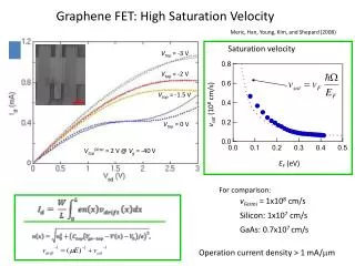
Current flows from metal into semiconductor : ( : area of contact , : constant ) Current flows from semiconductor to metal : ( : bias voltage ) Saturation current : For forward bias (+V) the net current increases exponentially with voltage. For reverse bias (-V) the current is essentially constant and equal to . The saturation current is about three orders of magnitude smaller than the forward current.
No conduction between source and drain • Switch is off MOSFET is a device used for amplifying or switching electronic signals. The threshold voltage of a MOSFET is usually defined as the gate voltage where an inversion layer forms at the interface between the insulating layer (oxide) and the substrate (body) of the transistor. • Gate attracts electrons, including an n-type conductive channel in the substrate below the oxide • Electrons flow between n-doped terminals • The switch is on
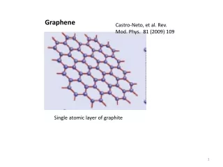
Graphene is a one-atom-thick planar sheet of carbon atoms that are densely packed in a honeycomb crystal lattice. The name comes from graphite + -ene; graphite itself consists of many Graphene sheets stacked together. In Graphene electrons / holes are confined to a plane of atomic thickness. This makes Graphene devices sensitive to the surrounding environment such as substrate and the dielectric media in contact with Graphene. Graphene
Graphene-FET Metal electrodes : Ti Distance between source and drain : 5 um The center of the device was exposed to each solvent. After measurement, the solvent was removed and dried with Nitrogen gas. The source – drain bias was kept constant at 10 mV.
Dielectric Screening Effect Minimum position : Dirac point On both sides of Dirac point, the conductivity increases linearly with the carrier density and then slows down. Eventually, it approaches a constant conductivity.
The role of charged impurities The scattering by charged impurities leads to a linear dependence of conductivity on carrier density. In addition charged impurities are believed to generate potential fluctuations that create electron and hole puddles in Graphene. : residual density – determines the conductivity of Graphene and also responsible for observed finite conductivity at Dirac point. ( : impurity concentration , : coupling strength of dielectric , : normalized voltage fluctuation correlation ) calculations predict that the density of effective charged impurities reduces as increases and the induced scattering in Graphene decreases accordingly.
Mobility Slopes of linear regions on both sides of the conductivity minimum : electron / hole mobility in each dielectric medium : back gate capacitance a) Both hole mobility (filled circles) and electron mobility (empty circles) increase with (decreasing with ) before reaching a plateau value. (phonon scattering) b) Asymmetry factor isthe ratio of electron to hole mobilities and at high asymmetry in the electron and hole mobilities diminishes. This explains screening effect of charged impurities for scattering.
Dirac point changes : position of minimum conductivityand it is a function of , which reduces as increases. : width of minimum conductivity plateau decreases with . : magnitude of minimum conductivity decreases from 18 to 3.5 .
Summery Transport properties of Graphene FET in different dielectric solvents have been studied. Screening effect of charged impurities (esp. at high κ) improves device performance. Upon increasing the dielectric constant : Both electron and hole mobilities increase a few orders of magnitude The width of the conductivity minimum decreases sharply and approaches zero in high κ solvents. The position of minimum conductivity tend to shifts positively The minimum conductivity value decreases from 18 to 3.5 The conductivity saturation occurs at lower carrier densities , and the short range conductivity changes little
References : • Fang Chen, Jilin Xia; Nano Lett. Vol. 9 , No. 7 , 2571 – 2574 (2009) • Rolf E. Hummel; Electronic Properties of Materials; Springer; New York; Third Edition; 2000