TPS92691 SEPIC LED DRIVER SIMULATION
100 likes | 138 Vues
Consultation for optimizing TPS92691 SEPIC LED driver, analyzing simulations, reducing current ripple, and improving ramp-up delays. Addressing design queries and calculations.

TPS92691 SEPIC LED DRIVER SIMULATION
E N D
Presentation Transcript
TPS92691 SEPIC LED DRIVER SIMULATION Requirement: 1. To drive 3 LEDs (SFH4725AS) in Series and total Forward Voltage 12.7V. 2. To drive minimum Current 200mA and maximum current 3A 3. Battery minimum voltage 7.4V, Nominal Voltage 12V and Maximum Voltage 18.5V
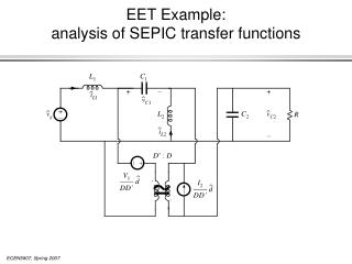
TPS92691 Sepic LED Driver Schematics No Soft start Capacitor PWM:
1. VIADJ:2.1V for ILED 3A • 1st Plot : PWM • 2nd Plot: Output LED Current • 3rd Plot: Coupled inductor Primary current , Secondary current • 4thPlot: Gate Voltage • Observations: • I. 11A ripple (20uS) on L2(Primary side) is coming during 1st PWM ON • 3.25A is output current ramp up and than Stable for 3A. • Output current ramp up after 600us of PWM • Gate is switching on as soon as first PWM ON so 11A ripple is coming
VIADJ:2.1V for ILED 3A Cont.….. 1st Plot : PWM 2nd Plot: Output LED Current 3rd Plot: Gate Current 4thPlot: Gate Voltage 1st Plot : Gate Voltage 2nd Plot: Coupled Inductor Primary and Secondary
2. VIADJ:1.05V for ILED 1.5A • 1st : PWM • 2nd : Output LED Current • 3rd : Gate Voltage • 4th : Coupled inductor Primary current , Secondary current • Observations: • 9.5A ripple ion L2 (Primary side) s coming during 1st PWM ON • 1.85A is output current ramp up and than Stable for 1.5A • Output current ramp up after 1ms in 1st PWM..
3. VIADJ: 0.14 V for ILED 200mA • 1st : LED Forward Voltage • 2nd : PWM • 3rd : Output LED Current • 4th : Coupled inductor Primary current , Secondary current • Observations: • 8A ripple on L2 (Primary side) is coming during 1st PWM ON • 350mA is output current ramp up and than Stable for 200mA • No output current for 2 PWM pulses, it will ramp up after 200us of 3rd PWM
VIADJ:0.14V for ILED 200mA Cont.….. 1st Plot : PWM 2nd Plot: Output LED Current 3rd Plot: Gate Voltage 4thPlot: Coupled Inductor Primary current 1st Plot : MOSFET Q1 current 2nd Plot: Coupled Inductor Primary and Secondary
VIADJ vs. ILED As per simulation we need Coupled inductor 10uH with 12A DC current , N-CH MOSFET 15A
Queries • No Sepic calculation formulas in datasheet, Please specify which document to consider for Design calculations. • 2. We have used “AN-1484 Designing A SEPIC Converter” for design calculations, please confirm whether is this correct document? • 3. Gate is switching ON as soon as PWM is ON, due to this 11A ripple is coming in 20us. Please let us know how to avoid this. • 4. As per calculation the Primary and Secondary current is 6.2A+3.6A=9.8A but we have observed in 11A in primary side itself, Please advise how to reduce this. • 5. From Output high Current 3A to Low Current 200mA, Output LED current ramp up is getting delay. 3A – 600us in 1st PWM, 1.5A – 1ms in 1st WPM and 200mA -2 PWM and 200us in 3rd PWM. Please advise how to reduce this delay?
THANK YOU www.hcl.com