Download
1 / 18
210 likes | 389 Vues
Fanout in Quantum-dot Cellular Automata. Kameshwar K. Yadavalli, Alexei O. Orlov, Ravi K. Kummamuru, John Timler, Craig Lent, Gary Bernstein, and Gregory Snider Department of Electrical Engineering University of Notre Dame Supported by DARPA, NSF, ONR, and W. Keck Foundation. Outline.

E N D
Fanout in Quantum-dot CellularAutomata Kameshwar K. Yadavalli, Alexei O. Orlov, Ravi K. Kummamuru, John Timler, Craig Lent, Gary Bernstein, and Gregory Snider Department of Electrical Engineering University of Notre Dame Supported by DARPA, NSF, ONR, and W. Keck Foundation
Outline • Quantum Cellular Automata paradigm • Initial devices • Clocked QCA • Power Delay Product • Metal tunnel junction implementation • QCA latch • QCA shift register • Fanout in QCA • Summary
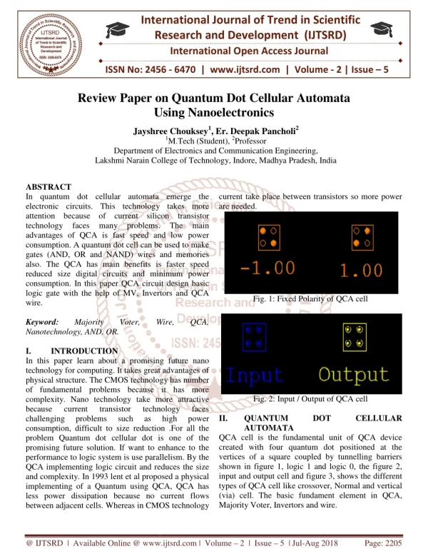
A cell with 4 dots 2 extra electrons and inter-dot tunneling Polarization P = -1 Bit value “0” Quantum-dot Cellular Automata Information encoded in charge configuration Polarization P = +1 Bit value “1” Neighboring cells tend to align by Coulombic coupling QCA simulations are available at www.nd.edu/~qcahome/ Polarization P = 1 Bit value “1”
A M B C A 0 0 0 0 1 1 1 1 B Out C Initial QCA devices Majority gate Binary wire Inverter • Ground state computation • Possibility of metastable states • Lack of power gain and signal level degradation Programmable 2-input AND or OR gate.
Benefits of Clocked QCA • Power Gain. Energy is supplied directly to cells by the clock, not by the signal inputs alone. • Pipelined Architectures. Clocked cells in locked state acts as a memory controlled by the clock. A large QCA array can be divided into sub-arrays using phase shifted clocks. • Fanout in QCA.A single latch can drive multiple latches to create a complex circuit. • Adiabatic clocking with reversible computation can beat the limit of power dissipation per bit operation, kTln2.
P= +1 P= –1 Null State Implementation of Clocking in Quantum-dot Cellular Automata Semiconductor dots: Clocking achieved by modulating inter-dot barriers Metallic or molecular dots: Clocking achieved by modulating the energy of a third dot • Lent et al., Physics and Computation Conference, Nov. 1994 • Likharev and Korotkov, Science 273, 763, 1996 Clock signals need not have to be sent to individual cells, but to sub-arrays of cells.
energy x Clocking in QCA Keyes and Landauer, IBM Journal of Res. Dev. 14, 152, 1970 Initial State With clock applied 1 0 Clock Input removed Clock barrier is slowly raised Null State 0 but Information is preserved! Clock Applied Differential Input applied 0
Switching Energy in QCA Quasi-adiabatic operation of QCA devices leads to very low power dissipation.
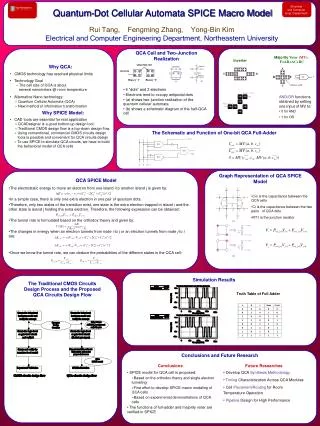
A -VIN -VIN Vg ~ +VIN +VIN +VIN +VIN QCA Latch: A Building Block The third, middle dot acts as an adjustable barrier for tunneling Electrometer SET D1 D1 MTJ MTJ D2 D2 MTJ MTJ D3 D3 1mm MTJ=multiple tunnel junction SEM Micrograph of a QCA latch
Weak input signal sets the direction of switching Clock drives the switching Memory Function demonstrated Inverter Function demonstrated Latch -VIN D3 VCLK D2 +VIN “High” D1 E1 SET electrometer Experiment: Single-Electron Latch in Action T=100 mK Input Clock Switch to “0” Hold “1” Switch to “neutral” Switch to “neutral” Hold “0” Switch to “1”
CC D1 D4 CC D2 D5 1mm CC D3 D6 CC QCA Two-Stage Shift Register • Two latches with two electrometers for readout • Inter-latch coupling by means of inter-digited capacitors (CC) • A Two-phase Clock to control electron switching is used • One latch serves as input for the other SEM micrograph +VIN VCLK1 VCLK2 -VIN
Operation of QCA Shift Register • Small external input applied – SR remains in neutral state • CLK1 applied 1st latch switches. Input now can be removed • CLK2 applied 2nd latch switches • Process is repeated for the inverted input +VIN VCLK1 VCLK2 -VIN
NULL CLK2 CLK1 CLK1 + Input - NULL Fanout in QCA Writing Information into first stage latch Transfer information into second stage latches
Fanout in QCA allows for complex circuits to be designed and operated. A latch in the first stage (L1) is coupled to two latches (L2, L3) in the second stage. A two phase clock (VCLK1, VCLK2) controls information transfer between the two stages. Information is first written into L1, then clocked into L2, L3 on the application of VCLK2. SET E1 L2 L1 e SET (E2) +VIN/2 e VCLK1 VCLK2 -VIN/2 e SET E4 L3 E3 SET Fanout in QCA
Operation of Fanout in QCA • All the latches are initially in null state. • A differential input is then applied to L1, to define the polarization state. • On the application of VCLK1, electron switches in L1 and is locked after the input is removed. • VCLK2 is then applied to L2, L3, with the locked state of L1 providing the input to L2, L3. • Information from L1 is written to L2 and L3.
QCA with Fanout • An implicit demonstration of power gain and the benefit of clocking. • In the absence of clocking, there will be signal level degradation in a fanout gate. • Also, the middle latch will see two kinks resulting in a higher energy state, stopping the computation. • As the second stage latches are driven by a weak input, the power gain in the second stage latches is greater than unity. Kinks • Enables multi-tasking architecture. • Affords the creation of complex circuitry.
Summary • Clocked QCA offers a working paradigm for digital nanoelectronics in the quantum realm: • orders of magnitude lesser power dissipation than FETs • power gain for signal level restoration • pipelining • Latch and shift register elements for information processing • Fanout gate in QCA paradigm is demonstrated • Future Work: Molecules? High resistive junctions for QCA latches in place of MTJs, for higher charging energy • Future Work: High speed measurements on QCA
Fabrication of Metal-dot QCA cells Simple 4-dot cell is shown No clocking yet! • Dots = small metal (Al) islands separated by tunnel junctions (Al203) • Junctions: area of about 100 x 100 nm2 ; thickness is 0.1-0.5 nm • Charging energy is small, so that operation temperature is low (<1K) • High yield and good reproducibility allows proof of concept demonstration