Exploring Power Supply Topologies: Buck, Boost, and SEPIC Modules for EE Board
10 likes | 134 Vues
This module project designed by Christopher Stone, Christina Ells, and Sean Mounts aims to create educational tools showcasing various power supply topologies: buck, boost, and SEPIC. Integrated with the Digilent Electronics Explorer Board, these modules will allow students to adjust inductive and capacitive components via jumpers for hands-on learning. Users can evaluate each topology's performance, including noise, latency, and efficiency by modifying parameters. The modules serve as both teaching instruments and practical experiments in power electronics.

Exploring Power Supply Topologies: Buck, Boost, and SEPIC Modules for EE Board
E N D
Presentation Transcript
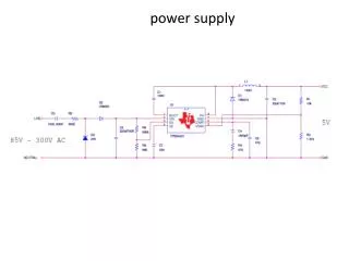
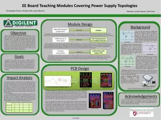
EE Board Teaching Modules Covering Power Supply Topologies Christopher Stone, Christina Ells, Sean Mounts Mentors: Scott Hanson, Clint Cole Module Design Background Adjustable Reactive Components? Jumpers Solution Objective This is a circuit representation of a buck power topology. It is meant to convert the voltage Vin into a lesser voltage using the inductor and capacitor so that it will match the Vout requirements of the system that is using it. It also uses a transistor and diode as switches in order to transition between connecting the inductor to the source in order to store energy, and the load to dissipate energy. All topologies must have adjustable inductive and capacitive values. To solve this issue a set of inductors/capacitors will be set up in parallel with a jumper in series with each one. By connecting contacts at each jumper and even doing combinations of them in parallel, different values can be achieved. Digilent needs a set of modules that will demonstrate a set of power supply topologies so that they may be used in future power electronics courses. The modules will demonstrate the buck, boost, and SEPIC and be compatible with Digilent’s Electronics Explorer Board. These modules will allow for the users to gauge the strengths as well as the weaknesses of each power supply topology by adjusting not only the loads, but the reactive components of each module (i.e. Inductors and capacitors). These modules will function as teaching tools for the user so that they may not only see how each power supply topology works but also how it loads and input voltage affect it’s noise, latency, and efficiency. PWM control of switch gate? Switching Regulators w/ Feedback Resistors Solution Buck Topology Output voltage control is a key design aspect of all the suggested topologies as it is the key component to a user’s understanding of the topology. Basic analysis of the each topology shows a relationship to duty cycle, however letting the user directly control that aspect seemed to overcomplicate. By using a prepackaged switching regulator the voltage can simply be controlled through a feedback network (i.e. a high resistance voltage divider). This feedback network would be controlled by the student using a variable resistor connected from the EE board itself. The boost topology is the opposite of the buck topology in that it steps the output voltage up so that it can be used in applications such as rectifiers and DC generators. It uses the capacitor to store the energy and dissipate it at a more normal rate in order to reduce any rippling in the voltage that may occur. Bottom Mounted Jumper Pins EE Board Compatibility Solution Boost Topology Goals All topologies must be able to mount the Electronics Explorer Board to allow for easy measurements and analysis of data. This issue was easily resolved by using a two single-row jumper pins and mounting them to the bottom of the board with enough spacing between them to accommodate the pin spacing of the EE Board. Doing so will provide a snug fit and all the nodes that require user interaction can be connected via these jumper pins. A SEPIC power topology is one that function like a buck and boost topology in that it converts the output voltage so that it can be less than, greater than or equal to the input voltage and is controlled by the duty cycle of the transistor. It is useful for applications in which the input voltage may vary while the output voltage needs to remain constant. This setup also differs from a buck-boost setup in that it keeps the output voltage positive. The goal of this project was to create a module for each topology that would not only simulate their function, but also allow for the user to be able to modify almost every parameter in order to see how they affect performance. The modules will not only be effective teaching tools, but also be user friendly. Since the user needs to understand what each topology does, the easier it is to interact with the faster the user can better understand the topology. SEPIC Topology PCB Design A duty cycle is defined as the duration of the event in a signal over the entire period of the signal, or in the case of the power supplies how long it takes to turn on and off. By changing how long a power source is considered “active” it is possible to change the duty cycle. Impact Analysis Digilent’s Electronics Explorer (EE) Board is essentially a “smart breadboard”. Through a USB connection and software, signals can be generated, measured, and analyzed right from the user’s computer. Draw Copper Traces and Planes Convert to Board Since these modules are required to be run on Digilent’s EE board, this would require the user to not only purchase the modules but if they have not already done so an EE board as well. While this does make the cost for learning and testing the power supply topologies much higher, it still gives the user a valuable insight into how each of the topologies work. By using these modules to test the noise, latency and efficiency of each power supply topology, they will be able to determine which power supply topology is most effective for various situations. This knowledge will help to lower unnecessary taxation on the environment and therefore reduce the wasted materials. It will also allow for users such as students to understand the requirements of the system they are working with better and therefore should be able to reduce the costs of building devices that rely on these power supply topologies such as cell phones and laptop computers. Electronics Explorer (EE) Board Schematic of the Buck topology designed by Team Dean Buck Board with components optimally arranged Finished Buck Board All three circuit diagrams were obtained from the Texas Instruments Power Supply Topology poster, “http://dc417.4shared.com/doc/OoBfQonF/preview.html” The EAGLE software was used in order to translate the buck, boost, and SEPIC design into something that could be interpreted by a PCB manufacturing company. First, a schematic with all the necessary components and their interconnections were created. Then, a board drawing would be created from these parts and it is the job of the designer to arrange components and connect traces as appropriate. There are many inherent rules associated with PCB design that must be followed in order to not only to make the resulting board work, but keep it from being sent back by the manufacturing company. As far as our design is concerned, these rules need to be taken into account considering the module designs we came up with. The most important rule is that the copper traces that connect each component together be wide enough to accommodate the maximum amount of current that could flow through them. A maximum current rating of 1.5A from the EE board could be assumed for most traces throughout the board and calls for about 56 mil width on these traces. However, most cases allowed for the use of planes which introduces a large conducting surface that connects all component parts of a particular node. This provided decreased resistivity for all cases. Acknowledgements Team Dean would like to acknowledge Clint Cole, Scott Hanson, and Gene Apperson for their guidance on this project, as well as Dr. Ali Mehrizi-Sani for PSCAD simulation assistance. We would also like to acknowledge Digilent Inc. and the WSU facilities for their support. Finished Boost Board Finished SEPIC Board Team Dean