MOSFET ID-VGS Characteristic and Circuit Models
240 likes | 359 Vues
This outline discusses the ID-VGS characteristic of MOSFETs, including the resistive switch model and small-signal model. It also covers the different regions of operation and the measurement of VT.

MOSFET ID-VGS Characteristic and Circuit Models
E N D
Presentation Transcript
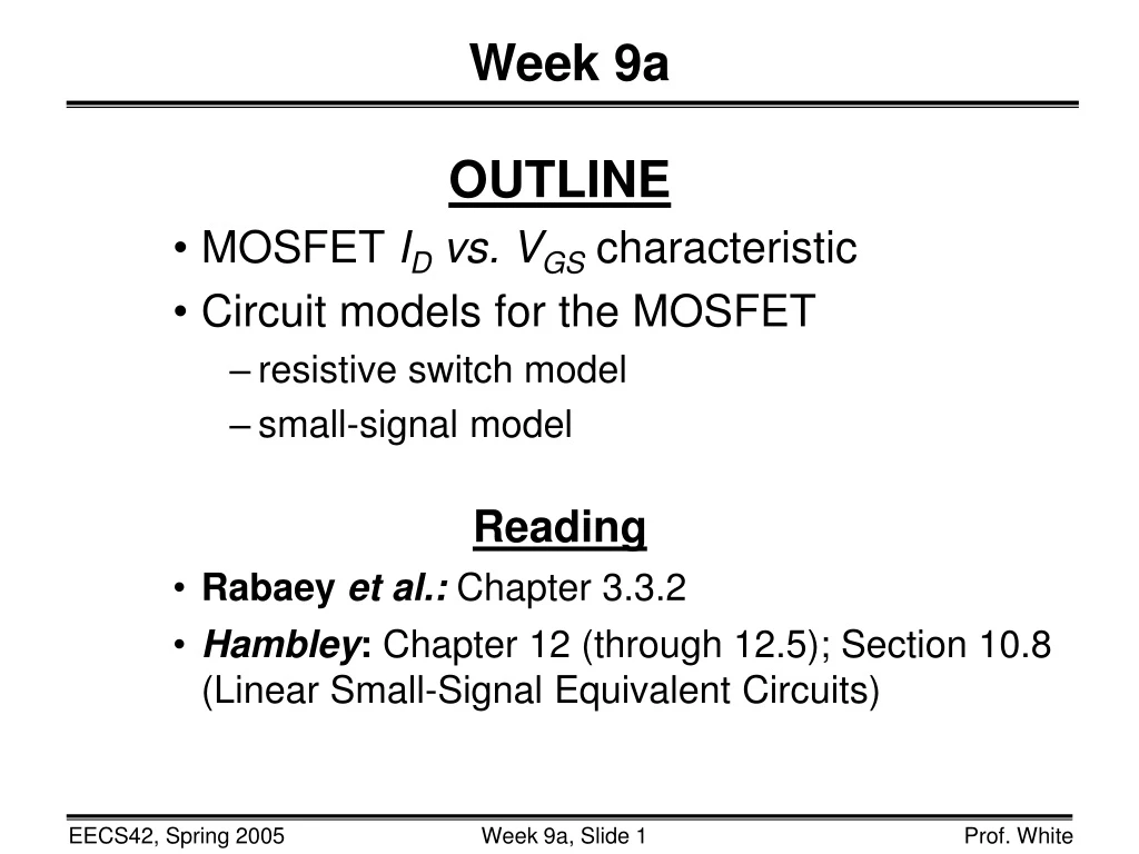
Week 9a OUTLINE • MOSFET IDvs.VGS characteristic • Circuit models for the MOSFET • resistive switch model • small-signal model Reading • Rabaey et al.: Chapter 3.3.2 • Hambley: Chapter 12 (through 12.5); Section 10.8 (Linear Small-Signal Equivalent Circuits)
IDvs.VDS Characteristics • The MOSFET ID-VDS curve consists of two regions: • 1) Resistive or “Triode” Region: 0 < VDS < VGS VT • 2) Saturation Region: • VDS > VGS VT process transconductance parameter “CUTOFF” region: VG < VT
Overview of NMOSFET Regions • Cutoff region: • Conditions: VGS < VT, any value of VDS • ID = 0 • Linear (or Resistive, or Triode) region: • VGS > VT, (VGS – VT) > VDS • ID = (f1 x f2 x f3 )VDS where • f1 = mCox (depends on the fabrication process) • f2 = W/L (chosen by the design engineer) • f3 = f3(VGS, VT, VDS) = [VGS – VT – VDS/2] • ~ (VGS – VT) if (VGS – VT) >> VDS /2 • Saturation region: • VDS > (VGS – VT) = VDSaturation2= (VGS – VT)2 • ID = (1/2) f1 x f2 x (VGS – VT)2
MOSFET IDvs.VGS Characteristic • Typically, VDS is fixed when ID is plotted as a function of VGS Long-channel MOSFET VDS = 2.5 V > VDSAT Short-channel MOSFET VDS = 2.5 V > VDSAT
MOSFET VT Measurement • VT can be determined by plotting IDvs.VGS, using a low value of VDS : ID (A) VGS (V) 0 VT
Subthreshold Conduction (Leakage Current) • The transition from the ON state to the OFF state is gradual. This can be seen more clearly when ID is plotted on a logarithmic scale: • In the subthreshold (VGS < VT) region, This is essentially the channel- source pn junction current. (n, the emission factor, is between 1 and 2) (Some electrons diffuse from the source into the channel, if this pn junction is forward biased.) VDS > 0
Qualitative Explanation for Subthreshold Leakage • The channel Vc (at the Si surface) is capacitively coupled to the gate voltage VG: Using the capacitive voltage divider formula: DEVICE CIRCUIT MODEL VG VG VD n+ poly-Si Cox + Vc – n+ n+ Cdep The forward bias on the channel-source pn junction increases with VG scaled by the factor Cox / (Cox+Cdep) Wdep depletion region p-type Si
Slope Factor (or Subthreshold Swing) S • S is defined to be the inverse slope of the log (ID) vs.VGS characteristic in the subthreshold region: VDS > 0 Units: Volts per decade Note that S≥ 60 mV/dec at room temperature: 1/Sis the slope
VT Design Trade-Off(Important consideration for digital-circuit applications) • Low VT is desirable for high ON current IDSAT (VDD - VT) 1 < < 2 where VDD is the power-supply voltage …but high VT is needed for low OFF current log IDS Low VT High VT IOFF,low VT IOFF,high VT VGS 0
The MOSFET as a Resistive Switch • For digital circuit applications, the MOSFET is either OFF (VGS < VT) or ON (VGS = VDD). Thus, we only need to consider two ID vs. VDS curves: • the curve for VGS < VT • the curve for VGS = VDD ID VGS = VDD (closed switch) Req VDS VGS< VT(open switch)
Equivalent Resistance Req • In a digital circuit, an n-channel MOSFET in the ON state is typically used to discharge a capacitor connected to its drain terminal: • gate voltage VG = VDD • source voltage VS = 0 V • drain voltage VD initially at VDD, discharging toward 0 V The valueof Req should be set to the value which gives the correct propagation delay (time required for output to fall to ½VDD): Cload
V + dd V + dd = = Figure 0.1 CMOS circuits and their schematic symbols
Typical MOSFET Parameter Values • For a given MOSFET fabrication process technology, the following parameters are known: • VT (~0.5 V) • Coxand k (<0.001 A/V2) • VDSAT ( 1 V) • l ( 0.1 V-1) Example Req values for 0.25 mm technology (W = L): How can Req be decreased?
P-Channel MOSFET Example • In a digital circuit, a p-channel MOSFET in the ON state is typically used to charge a capacitor connected to its drain terminal: • gate voltage VG = 0 V • source voltage VS = VDD (power-supply voltage) • drain voltage VD initially at 0 V, charging toward VDD VDD 0 V iD Cload
Common-Source (CS) Amplifier • The input voltage vs causes vGS to vary with time, which in turn causes iD to vary. • The changing voltage drop across RD causes an amplified (and inverted) version of the input signal to appear at the drain terminal. VDD RD iD vs + vOUT = vDS + + vIN = vGS + – VBIAS
Notation • Subscript convention: • VDSVD– VS , VGS VG– VS , etc. • Double-subscripts denote DC sources: • VDD , VCC , ISS , etc. • To distinguish between DC and incremental components of an electrical quantity, the following convention is used: • DC quantity: upper-case letter with upper-case subscript • ID , VDS , etc. • Incremental quantity: lower-case letter with lower-case subscript • id , vds , etc. • Total (DC + incremental) quantity: lower-case letter with upper-case subscript • iD , vDS , etc.
Load-Line Analysis of CS Amplifier • The operating point of the circuit can be determined by finding the intersection of the appropriate MOSFETiDvs.vDS characteristic and the load line: iD (mA) load-line equation: vGS (V) vDS (V)
Voltage Transfer Function (1): transistor biased in cutoff region (2): vIN > VT; transistor biased in saturation region (3): transistor biased in saturation region (4): transistor biased in “resistive” or “triode” region vOUT Goal: Operate the amplifier in the high-gain region, so that small changes in vIN result in large changes in vOUT vIN
Quiescent Operating Point • The operating point of the amplifier for zero input signal (vs = 0) is often referred to as the quiescent operating point. (Another word: bias.) • The bias point should be chosen so that the output voltage is approximately centered between VDD and 0 V. • vs varies the input voltage around the input bias point. Note: The relationship between vOUT and vIN is not linear; this can result in a distorted output voltage signal. If the input signal amplitude is very small, however, we can have amplification with negligible distortion.
Bias Circuit Example VDD RD R1 R2
Rules for Small-Signal Analysis • A DC supply voltage source acts as a short circuit • Even if AC current flows through the DC voltage source, the AC voltage across it is zero. • A DC supply current source acts as an open circuit • Even if AC voltage is applied across the current source, the AC current through it is zero.
NMOSFET Small-Signal Model D G id + vgs + vds gmvgs ro S S transconductance output conductance
Channel-Length Modulation • If L is small, the effect of DL to reduce the inversion-layer “resistor” length is significant • ID increases noticeably with DL (i.e. with VDS) ID ID= ID(1 + lVDS) l is the slope ID is the intercept VDS
Small-Signal Equivalent Circuit G D + vout + vin + vgs gmvgs R1 R2 RD ro S S voltage gain