
Enhancements in Motherboard 4: From Digital Drivers to Improved OPAMP Performance
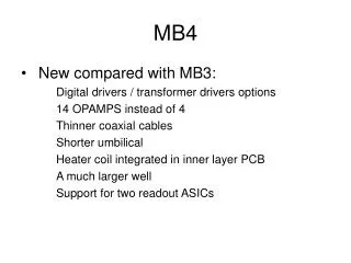
The Motherboard 4 (MB4) series introduces significant advancements over its predecessor MB3, transforming driver technology with digital drivers and increased OPAMP capacity. MB4 integrates 14 OPAMPs instead of 4, utilizing thinner coaxial cables, a compact umbilical design, and an inner-layer PCB with an integrated heater coil. This model enhances performance with dual readout ASIC support and addresses noise issues experienced in earlier versions. Key changes span from improved driver configurations to optimized power routing, ensuring better signal integrity and reduced interference.

Enhancements in Motherboard 4: From Digital Drivers to Improved OPAMP Performance
E N D
Presentation Transcript
MB4 • New compared with MB3: Digital drivers / transformer drivers options 14 OPAMPS instead of 4 Thinner coaxial cables Shorter umbilical Heater coil integrated in inner layer PCB A much larger well Support for two readout ASICs
Motherboard 4 series • Quick history • Motherboard 4.2 noise issues.
Versions • MB4.0 September 2005: • Transformer drive. • MB4.1 December 2006: • As 4.0 but with corrected CCD footprint • MB4.2 March 2006 • As 4.1 but with digital driver • MB4.3 Expected mid July • Many corrections implemented
Noise issues Motherboard 4.2 Behaviour of the OPAMPS Transmission of digital clock signal across the well Lack of de-coupling gnd1 to gnd2 Bringing in power to the driver IC
Behaviour of the OPAMPS • 3 dB bandwidth ~ 125 MHz • Essentially independent from source resistance • No overshoot in the frequency characteristic • OPAMP + resistor noise estimated at 100µV with ~4kΩ source impedance (this was not measured precisely) (source impedance with CCD connected should reduce the resistor noise to ~40µV)
Transmission of digital clock signal across the well • The two phases of the clock signal cross the well (inputs to drivers). As the gnd1 plane is broken under the well, the return current has to find a circuitous route back. The resulting ground bounce can be observed in the OPAMP signals. (~20mVpp)
Lack of de-coupling gnd1 to gnd2 • As we usually de-couple to ground it was not realised that in case of multiple grounds we need to decouple the grounds to each other. Adding coupling capacitors between these planes reduced the amount of ringing on them and changed the frequency of the ringing from 10MHz to 50MHz.
Bringing in power to the driver IC Following tests on motherboard 4.3 we conclude: We must isolate the driver return line from the motherboard ground, so that the noisy driver return current doesn’t affect the OPAMP ground. To do this, it may be best to bring in the driver supply to the driver on a strip line minimising the travel of its power supply through the PCB. Furthermore multiple vias need to be used to connect this strip line and decoupling capacitors to the driver. Low inductance capacitors should be used. The use of a strip line should minimise magnetic fields caused by the driver supply current. For the case of the single metallised CCD there will inevitably always be a substantial current from one side of the CCD to the other. This will continue to cause interference on the board. For the double metallised CCD there are connections to both CCD phases on each side, which minimises the return path for the clock current.
MB 4.3 lay-out checks • ID and RG pulse signals expected to couple badly. We will aim to turn connections into strip line if possible.
MB4.3 checks • Increase OPAMP immunity to noise by turning ground plane/power plane areas under OS Opamps into islands connected to the main planes via one place only