Efficient Asynchronous Protocol Converters for Two-Phase Delay-Insensitive Global Communication
Efficient Asynchronous Protocol Converters for Two-Phase Delay-Insensitive Global Communication. Amitava Mitra Intel Corp., Bangalore, India William F. McLaughlin Columbia University, Electrical Engineering Steven M. Nowick Columbia University, Computer Science. Outline.

Efficient Asynchronous Protocol Converters for Two-Phase Delay-Insensitive Global Communication
E N D
Presentation Transcript
Efficient Asynchronous Protocol Converters for Two-Phase Delay-Insensitive Global Communication Amitava Mitra Intel Corp., Bangalore, India William F. McLaughlin Columbia University, Electrical Engineering Steven M. Nowick Columbia University, Computer Science
Outline • Motivation and Contribution • System-on-Chip: Concepts and Trends • Asynchronous Signaling Styles • Target Asynchronous SOC Architecture • Contribution • Proposed System Architecture • Experimental Results • Extensions: Other Signaling Styles • Conclusions and Future Work
System-on-Chip (SOC): Concept and Trends • Microelectronic trends enabling SOC design • Increasing integration density + chip size • Formerly discrete functions (memory, I/O) now integrated • Popularity of “multi-core” designs • Heterogeneous SOC: • Large complex chip with broad functionality • Many independent computation nodes • Multiple cores, memories, accelerators, multimedia processing, etc. • Often includes multiple timing domains • Complex network-style interconnect fabric • Challenges in Heterogeneous SOC design: • Wire costs not scaling down with device size • Increasing proportion of power and delay in interconnect • Robust and high-performance interconnect design: • High latencies between remote nodes • Mixed timing, timing variability/uncertainty • Need to support varied components: modular/scalable design
SOC Communication Fabric • Growing factor in overall system performance • Ideal Requirements: • Speed: high throughput, low latency • Low power • Robust to timing variations • Flexibility: integrate modular IPs and upgrades • Asynchronous design well-suited to these goals • Timing robust flexible designs • Lower power than synchronous • Work by Quinton, Greenstreet, and Wilton [ICCD 2005] • GALS-style: • global LEDR interconnect + local synchronous blocks • does not provide details of protocol converters
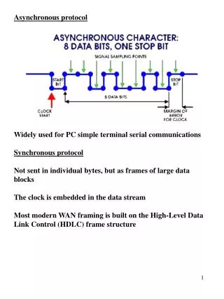
Asynchronous for SOC Communication • Advantages of asynchronous global communication • Delay-insensitive (DI) encoding • Removes timing constraints on global routing • No clock signals to route across chip • Significant power advantage • Can support both async + sync computation • Delay-insensitive async logic combats growing variability concerns • GALS style: Globally-Asynchronous Locally-Synchronous • Several popular async signaling protocols • Dual rail four-phase, LEDR, 1-of-4, bundled data, others • No single protocol ideal for both logic and communication
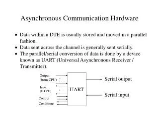
Background: LEDR Signaling • Dual-rail encoding: two wires per bit – delay-insensitive • “Level-encoding”: • Data rail: holds actual data value • Parity rail: holds parity value • Alternating-phase protocol: • Encoding parity alternates between odd and even Bit value LEDR Encoding data rail parity rail Phase
LEDR Signaling • Exactly one wire transition for each new data item Data rail: carries bit value in both phases 0 1 0 0 1 1 1 data parity even odd even odd even odd even Parity rail: phase alternates with each data item
Four-Phase Dual-Rail Signaling • Alternative DI Code • Key Differences: • Four-phase (Return-to-Zero) protocol • Spacer (reset) state required between each data item • One-hot encoding: • True rail (encodes 1) & false rail (encodes 0) 1 0 1 1 Data values True rail False rail Evaluation (one rail high) Reset (both rails low)
Four-Phase Dual-Rail vs. LEDR • Advantages of four-phase dual-rail: • Delay-insensitive logic using standard gates • Implementations are simple and fast: widely used • LEDR: complex & impractical • Disadvantages of four-phase dual-rail: • System-level communication throughput: • Spacer state doubles round-trip communication latency • LEDR: no spacer required • Power dissipation: • Two transitions/bit (up and down) for each data item • LEDR: only one transition/bit • Conclusion: • Four-phase dual-rail better for implementing function blocks • LEDR is better for global communication
Target Asynchronous SOC Architecture • Three major components: • Global communication network (LEDR) • Local computation nodes (varied styles) • New requirement: protocol converters at interfaces • Allow full separation of computation and communication Our goal – Protocol converters to enable this global LEDR SOC
Contribution • High-speed protocol converters to enable heterogeneous SOC architectures • Supports high-throughput, robust global communication • LEDR encoding • Supports efficient design of local function blocks • (i) 4-phase dual-rail, (ii) 1-of-4, (iii) single-rail bundled data • Features: • Family of low-latency protocol converters: • support above 3 local encoding styles • High throughput: • facilitates concurrent interaction of nodes • Timing-robust: • converters almost entirely QDI • Low design effort: • standard cell design flow • Fully implemented in 0.18 μm CMOS • Layout and simulation • FIFO throughputs up to 250 MHz
Two Target SOC Topologies 1. “Pipeline-style” topology • Feed-forward data path: • uni-directional token flow • Receiving node returns a single ACK (control signal) • Supports concurrency between nodes Data feeds forward Acknowledge sent back
Two SOC Topologies (cont.) 2. “Server-style” topology • Client passes data token to server • Server computes/returns data token to client (result) • Explicit ACK unnecessary • Proposed SOC architecture supports both topologies Four-phase server Four-phase data client Bi-directional data flow: data passed back to client on completion
Outline • Motivation and Contribution • Proposed System Architecture • Architecture Overview • System Simulation • Detailed Hardware Implementation • Timing Analysis • Experimental Results • Extensions: Other Signaling Styles • Conclusions and Future Work
Architecture Overview Four-phase core • External LEDR interface, internal four-phase core • Four-phase signals are shown in red • Two-phase or transition signals are shown in yellow LEDR input LEDR output
Control Signals • Two-phase control signals Phase of LEDR input (request from left) Phase of LEDR output (forward complete) Acknowledge to left neighbor Acknowledge from right neighbor
Control Signals • Four-phase control signals Completion detect four-phase evaluate and RZ Enable four-phase evaluate and RZ
System Simulation • LEDR inputs begin arriving at quiescent system LEDR inputs arrive Completion detection
System Simulation • Input completion detection sent to control All input phases matching Transition to new phase
System Simulation • Control enables four-phase evaluate phase Enable rises
System Simulation • LEDR input converted to four-phase Enable now high One wire of each four-phase pair rises
System Simulation • Four-phase function evaluation
System Simulation • Four-phase bits decoded to LEDR • Each bit converted as soon as it computes LEDR outputs to next node generated Four-phase complete not used in evaluate phase
System Simulation • LEDR output completion detection Output pairs ACK from right may come any time after all pairs are sent
System Simulation • Control enables four-phase reset phase Enable falls
System Simulation • Function block inputs return-to-zero • ACK is sent concurrently to left Enable now low Pipeline concurrency: request new data during reset phase
System Simulation • Four-phase reset propagates through logic block New data may arrive now that ACK has been sent Reset Completion detection Enable remains low
System Simulation • Four-phase reset completes • Complete internal cycle has now been performed Complete falls
System Simulation • New evaluate phase begins when Enable rises again • Pre-conditions: reset finished, new data REQ, and old data ACK Three-way synchronization Input phase transitions when new data ready ACK transitions when outputs safe to change Complete low (means reset finished)
Detailed Hardware Implementation • Each block implemented in CMOS standard cells • Design has few non-QDI timing constraints Four-phase core LEDR input LEDR output
Four-phase Encode (Input Converter) • Converts LEDR input to four-phase dual-rail • Enable=‘1’: outputs evaluate based on LEDR data • Enable=‘0’: outputs reset (LEDR data blocked)
Four-phase Decode (Output Converter) • Converts four-phase bits to LEDR output • LEDR data rail encoding • Assert either S (1 value) or R (0 value), then return-to-hold • More robust alternative: C-element
Four-phase Decode (Output Converter) • Converts four-phase bits to LEDR output • LEDR parity rail encoding • Parity output: based on 4-phase data and LEDR input phase (parity) • Alternating phases: green vs. red gates • D-latch: blocks new input parity arrival until 4-phase reset complete even phase odd phase
1-Bit Completion Detectors • LEDR CD at input and output • Four-phase CD in function block • Both protocols have one gate CD • XOR (parity) for LEDR • OR for four-phase dual-rail 1-bit LEDR completion detector 1-bit four-phase completion detector
N-Bit Completion Detectors • C-element trees • Used for both LEDR and four-phase • C-element: standard cell implementation (AOI222 w/feedback)
Control Block • Main Purpose: controls 4-phase function block • 4-phase eval requires 3-way synchronization • Function block: previous RZ complete • Primary inputs: new data arrival • Right interface (in pipeline): ACK received • In pipeline topology: also sends left ACK For pipeline topology only
Control Block • Converts two-phase inputs to four-phase outputs Two-phase to four-phase conversion
Control Block: Signaling Conversion Pulse-mode (timed) Transition-signal (falling or rising ) Four-phase (level-sensitive) SR latch captures the pulse Inverter and XNOR form simple pulse gen
Timing Requirements • Circuits almost entirely QDI • Exceptions: • Control block: • Two-sided timing constraint on length of pulse • Sensitive to both gate and wire delays • Careful layout required • Latches: simple hold time constraints • SR latches can be replaced by C-elements • C-elements also have implementation-specific timing constraints • SR latch much faster than our standard cell C-element • D latch can be removed at cost of concurrency
Outline • Motivation and Contribution • Proposed System Architecture • Experimental Results • Design Methodology • Datapath Setup • Simulation Results • Latency and Throughput Analysis • Extensions: Other Signaling Styles • Conclusions and Future Work
Design Methodology • Standard cell design flow with complete layout • 0.18 μm TSMC CMOS process • 4 metal layers of 7 available used in routing • Custom place-and-route used • Only major layout concern: pulse generator circuit • Design could be automated with constraints on pulse • Analog simulations: based on layout-extracted design • Test vectors including limiting fast and slow cases
Datapath Implementation • Two function blocks implemented • An 8x8 carry-save multiplier • An empty FIFO stage • FIFO contains four-phase completion detector only • Demonstrates minimum possible node latency • Blocks are QDI in evaluate, but “eager” in reset • Implemented in combinational CMOS • “DIMS”-style logic (with C-elements) could be used instead • QDI in both directions • Increases both forward and reverse latencies
Multiplier Layout • Includes dual rail multiplier and all conversion circuits • Total area of 0.051 mm2 • FIFO stage has area of 0.018 mm2
Performance Results 3 Metrics: • Forward Latency: input arrival output data available • Average Values: Multiplier:6.8 ns; FIFO:2.9 ns. • Stabilization Time: input arrival reset complete (circuit quiescent) • Multiplier:10.5 ns; FIFO:6.3 ns. • Pipelined Cycle Time: min processing time/data item (steady-state) • Multiplier:8.3 ns; FIFO4.0 ns.
Performance Analysis • Forward latency: overhead • 2.2 ns for both nodes • Overhead independent of function block size • Includes: • LEDR CD, control unit, input/output converters • Throughput: increased by concurrency • Benefit: 2.2 ns reduction in cycle time (vs. post-reset ACK) • Savings achieved even in environment without channel latency • “Core converter” overhead (no CD) extremely low • Only 1.1 ns average latency for converters + control • Completion detectors: • Account for half of forward latency overhead • Account for 55% of FIFO cycle time • Faster CDs would provide big improvement
Outline • Motivation and Contribution • Proposed System Architecture • Experimental Results • Extensions: Other Signaling Styles • Converters for 1-of-4 function blocks • Converters for bundled data function block • Conclusions and Future Work
Extensions to Other Local Protocols • Only small changes to handle 1-of-4 or bundled data • No change to control block • 1-of-4 encoding: • Input/output converters: • Small changes to logic • Needs standard 1-of-4 completion detector • Single-rail bundled data: • Input converter: not needed – use LEDR data rail • Output converter: • New basic circuit required (see paper for details) • Function block completion detection: • Use bundled ‘done’ signal • Asymmetric delay chain (fast reset)
Outline • Background and Motivation • Contribution • Proposed System Architecture • Experimental Results • Extensions: Other Signaling Styles • Conclusions and Future Work • Summary and Conclusion • Future Work
Summary and Conclusions • Support heterogeneous SOCs using hybrid protocols • LEDR: low-power, delay-insensitive communication fabric • Dual rail four-phase: Simple, fast logic blocks • Designed Converters for LEDR/four-phase SOC: • Low latency, high throughput, timing robust design • Robust concurrency system developed • Exploits four-phase reset to mask communication time • Simulations with realistic mid-sized function nodes • Demonstrated low latency overhead • Demonstrated low area overhead • Achieved throughputs up to 250 MHz for FIFO stage