Download
1 / 16
160 likes | 175 Vues
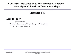
ECE 3430 – Introduction to Microcomputer Systems University of Colorado at Colorado Springs. Lecture #17 Agenda Today Output Compare Input Capture and Output Compare Examples MSP430 Timer Review. Timer Output Compare Function. Output Compare

E N D
ECE 3430 – Introduction to Microcomputer SystemsUniversity of Colorado at Colorado Springs Lecture #17 Agenda Today • Output Compare • Input Capture and Output Compare Examples • MSP430 Timer Review ECE 3430 – Intro to Microcomputer Systems Fall 2014
Timer Output Compare Function Output Compare - Sometimes it is desirable for a microcontroller to generate a precisely-timed digital waveform. Programmatically driving a waveform by repeatedly forcing a bit high and low will not yield a digital waveform with good integrity since the CPU can be interrupted at any time! - Some microcontrollers provide a feature called output compare which can be used to more accurately produce digital waveforms. - The MSP430 (G2553) provides 3 output compare channels per Timer_A module as part of the capture/compare timer block. - Each channel has a dedicated 16-bit output compare register. - A 16-bit value is loaded into the output compare registers. When TAR is equal to this value, an internal event is triggered. - When this internal event is triggered the output compare circuitry will alter the value on an output pin. These output pins can be associated with MSP430 external I/O pins (see device specific datasheet). - The output of each channel is called OUTx (OUT0, OUT1, and OUT2). - In all cases, P1DIR.x must be 1 (to make the I/O pin an output) and P1SEL.x must be 1 to disconnect the output from the normal CPU-controlled, general-purpose I/O and connect it to the timer. ECE 3430 – Intro to Microcomputer Systems Fall 2014
Timer Output Compare Function Output Compare Details- When the output compare generates an internal event (when the TACCRx register and TAR match), the OUTMODx bits in the TACCTLx register specify what to do to the respective output pin: ModeBit 7 Bit 6Bit 5 0 0 0 0 Output value in OUT bit (in TACCTLx as well) 1 0 0 1 Set 2 0 1 0 Toggle/reset3 0 1 1 Set/reset 4 1 0 0 Toggle 5 1 0 1 Reset 6 1 1 0 Toggle/set 7 1 1 1 Reset/set NOTES: * Modes 2, 3, 6, and 7 are only useful in up and up/down TAR count modes. * These modes are not useful for channel 0—since TACCR0 is used as the count threshold in up and up/down modes. * The first action is taken when TAR = TACCR1 and the second when TAR=TACCR0. ECE 3430 – Intro to Microcomputer Systems Fall 2014
Timer Output Compare Function Output Compare Details- The 16-bit output compare registers for each of the output compare channels are:Output Compare Channel 0 = TACCR0 Output Compare Channel 1 = TACCR1 Output Compare Channel 2 = TACCR2 - During output compare function, these registers are treated read/write by software! - When the TAR and TACCRx registers match, a “flag bit” (CCIFG) will be set in the appropriate TACCTLx register This flag only indicates that the registers matched and action has been taken on the associated output pin. It is set even if interrupts are disabled. - These flags can be cleared by writing a ‘0’ to the corresponding flag bit: CCIFG = 0 = flag cleared, waiting for output compare event (RESET state) CCIFG = 1 = flag set, output compare event occurred sometime in the past ECE 3430 – Intro to Microcomputer Systems Fall 2014
Timer Output Compare Function Output Compare Function (Optional Interrupt) (all of this is the same as it was for input capture) - Just as with the timer overflow, the flag getting set when action is taken against an output pin can generate an interrupt—however this is not a requirement! - Just like all MSP430 interrupts, each output compare channel has a relative priority. Output compare channel 0 has a higher priority than all the other output compare channels (see interrupt vector table in device-specific datasheet). - The timer overflow and compare channel 1 and 2 interrupts share an interrupt vector, so the source of the interrupt must be determined. The TAIV register can be used to do this expediently. TAIV is set to a distinct value based on the highest-priority, pending timer interrupt. The associated flag is automatically cleared by hardware. - Just like many other MSP430 interrupts, there is both a global and local interrupt mask involved: Global mask = GIE flag in the SR (this is a maskable interrupt) -> OK for CPU to acceptLocal mask = CCIE bit in appropriate TACCTLx register -> OK for timer to generate ECE 3430 – Intro to Microcomputer Systems Fall 2014
Timer Output Compare Function Output Compare Details- The CAP bit in the TACCTLx register must be set to 0 for compare mode—it is set to 1 only when the timer channel is used in input capture mode. - The OUT bit in the TACCTLx register can be set to force the timer-controlled output to either digital value (0 or 1)—provided the OUTMOD bits are all 0. This allows software to take control of the output pin at times if required. - Attempting to change the state of port pins under the control of an output compare channel using PxOUT will have no effect! The general-purpose port logic is disconnected from the output pin! - If trying to generate a periodic waveform by actively changing the TACCRx register in an ISR, the ISR must complete before TAR matches the new value of TACCRx. This would happen if you try to generate an arbitrarily high-frequency waveform. The CPU speed puts a limitation on the attainable frequency. ECE 3430 – Intro to Microcomputer Systems Fall 2014
Timer Output Compare Function Output Compare ApplicationsGenerate Square Waves - A square wave with a pre-defined duty cycle and frequency (period) can be generated. Useful in PWM control (motors).Generate Fixed Delay after Event - When an event occurs, we can trigger a specific # of “counts” after the event. Could also be an accurate delay subroutine.Generate a Pulse with a Certain Width - Trigger two ‘toggle’ output compares a certain count between edges. Event Output Compare TCNT ECE 3430 – Intro to Microcomputer Systems Fall 2014
Timer Output Compare Function (Example) Output Compare ExampleGenerate a square wave with a pulse width equal to TAR rollover on P1.2 (OUT1). OUT1 is the output from output compare channel 1. * Need to set P1.2 as an output and to use alternate function (timer-controlled). * Need to tell compare channel to toggle output. * Need to set up TAR in continuous count mode (leave at 1 MHz DCO-controlled). * Can optionally enable interrupts (for CPU notification) and provide ISR. Because we could configure the count threshold (by setting TACCR0 and switching to “up” TAR count mode), we can control the frequency of the 50% duty cycle waveform. We could also use “up/down” TAR count mode in combination with TACCR1 to create a waveform with a non-50% duty cycle. Roll Over Roll Over ECE 3430 – Intro to Microcomputer Systems Fall 2014
Timer Output Compare Function (Example) Output Compare Example Cont… ECE 3430 – Intro to Microcomputer Systems Fall 2014
Timer Input Capture Function (Example) Input Capture ExampleMeasure the frequency of a digital waveform provided on P1.2: Use CCI1A as the input to input capture channel 1. * Need to set P1.2 as an input and to use alternate function (routed to timer block). * Need to tell capture channel to look for rising (or falling edges). Both is overkill. * Need to set up TAR in continuous count mode (leave at 1 MHz DCO-controlled). * Can optionally enable capture interrupts (for CPU notification) and provide ISR. The captured TAR value will be in TACCR1 when the edge occurs. If we wanted to measure duty cycle too, we would need to look for both edges. For period/frequency only, either edge (but not both) would be sufficient. Period ECE 3430 – Intro to Microcomputer Systems Fall 2014
Timer Input Capture Function (Example) Should either avoid use of R4 and R5 from this point forward (used by ISR), or add do-no-damage to the ISR—a longer ISR increases the odds of a capture overflow (COV) and data loss. Period and PrevCap could reside in dedicated registers instead—but they would be off limits to this main code—faster but less flexible. Input Capture Example Cont… ECE 3430 – Intro to Microcomputer Systems Fall 2014
Timer Input Capture Function (Example) Input Capture Example Cont… ECE 3430 – Intro to Microcomputer Systems Fall 2014
Timer Review MSP430 Timer_A block The G2553 has two, three-channel Timer_A modules. They are referred to as Timer0_A3 and Timer1_A3. Each Timer_A register can be annotated with the Timer_A module instance number (required if not using instance 0). Ex) TA0R = TAR = timer register for Timer0_A3TA1R = timer register for Timer1_A3 TA0CCR0 = TACCR0 = capture/compare for instance 0, channel 0. TA1CCR0 = capture/compare for instance 1, channel 0. Main Timer - A 16-bit counter (TAR) that runs off of an internal or external clock source. It can trigger an interrupt upon overflow (return to 0x0000). The speed of the counter can be clocked down by a factor of 2, 4, or 8. The maximum count value can be established via a register (TACCR0). The counter can count in up/down mode. Input Capture – Used to capture external events via dedicated input pins. When the event occurs, the value of TAR is loaded into a pre-defined register (TACCRx). This is then used to calculate relative timing information between events. This can also cause an interrupt. Output Compare - Compare registers (TACCRx) are loaded with a 16-bit values. When TAR reaches the value in the register, an output compare trigger will occur. Upon the compare event, output pins on the MSP430 can be altered. This can also cause an interrupt. ECE 3430 – Intro to Microcomputer Systems Fall 2014
Timer Review The documentation will sometimes refer to the Timer_A block as: “Timer0_A3” or “Timer1_A3” In this example, 0 or 1 indicates the “instance” of Timer_A block in the MSP430. Our MSP430 (G2553) has two timer modules—but some (G2231) may have only one. In this example, 3 indicates that the Timer_A block contains three capture/compare channels—referred to as channels 0, 1, and 2. The channel 0 capture/compare register (TACCR0) serves an alternate purpose when the TAR is counting in “up” or “up/down” mode and, hence, cannot be used for typical compare/capture purposes in that scenario. If the TACCR0 is not needed to specify a threshold for this TAR count mode, it can be used for capture/compare purposes. All channels within a Timer_A instance share a common timer block (TAR). Independent Timer_A instances can be configured independently with potentially different clock domains. ECE 3430 – Intro to Microcomputer Systems Fall 2014
Timer Review The Timer_A peripheral registers are: TACCR0: Serves as count threshold in “up” and “up/down” mode—otherwise a typical compare or capture register for channel 0. TACCR1: Capture/compare register for channel 1. Software reads this during input capture and writes this during output compare. TACCR2: Capture/compare register for channel 2. Software reads this during input capture and writes this during output compare. TAR: The main timer (a 16-bit counter). Readable and writeable by software—but typically not modified by software. TACTL: The Timer_A “timer block” control register. Used to set up all the parameters of the “timer sub-block”. Does not specify the behavior of capture/compare timer blocks. TAIV: The Timer_A “interrupt vector generator”. An optional mechanism that expedites handling of timer interrupts (when more than one possible source is involved). This is a “reactive” register in that hardware state will change as a result of reading it (flags are cleared). TACCTL0/1/2: The channel 0/1/2 capture/compare configuration register. All input capture and output compare parameters are specified here. ECE 3430 – Intro to Microcomputer Systems Fall 2014
Timer Review The main timer (TAR) is normally left in continuous count mode for input capture. Specifying a roll-over threshold other than 0xFFFF can complicate math in some situations. Allowing the timer to run backwards further complicates things. These alternate count modes are more useful for output compare. The “up” and “up/down” count modes for TAR add much flexibility to the output compare system when generating a waveform. The combination of TAR clock source, TAR clock pre-scalar, and threshold allow tight control over the frequency of TAIFG (timer overflow events). The additional count modes also make changing the frequency or duty cycle of the output waveform (when using output compare) much easier. Generating periodic waveforms does not need to require periodic interrupts (and CPU servicing) thanks to these flexible count modes. ECE 3430 – Intro to Microcomputer Systems Fall 2014