Download
1 / 13
150 likes | 307 Vues
g4beamline study of Si PIN diode Bill Ashmanskas 2008-03-06. I didn't start until I got Camille's reminder email yesterday ... Nevertheless, I got something useful out of the simulation! So g4beamline is a pretty handy tool.

E N D
g4beamline study of Si PIN diodeBill Ashmanskas2008-03-06 • I didn't start until I got Camille's reminder email yesterday ... • Nevertheless, I got something useful out of the simulation! • So g4beamline is a pretty handy tool
Mean DE is 4 keV out of 660 keV. But in fact only 1% interact at all, and the ones that do interact seem to lose most of their energy. (Note that I measured energy lost by photon, not necessarily energy gained by silicon.) Not sure why a handful of E > 660 keV. preview of punchline ... stop here if you're bored
Ran 100K tracks in 2 minutes on a 6 year old PC (1.8 GHz P4)
I chose ASCII output; you could choose ntuple, root, etc. note that this is the output of a test run (1000 tracks), not the final run
match upstream & downstream particles; output consolidated data (e.g. DE in keV)
Mean DE is 4 keV out of 660 keV. But in fact only 1% interact at all, and the ones that do interact seem to lose most of their energy. (Note that I measured energy lost by photon, not necessarily energy gained by silicon.) Not sure why a handful of E > 660 keV.
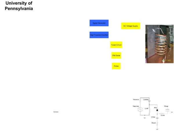
660 keV photons from Cs137 source • S1223-01 Hamamatsu silicon PIN diode • From datasheet: • Window 5.9mm, 1.3mm thick, borosilicate glass • Effective active area 3.6mm x 3.6mm • Egap 1.12eV at 25°C • From elsewhere • 316.5m intrinsic region thickness