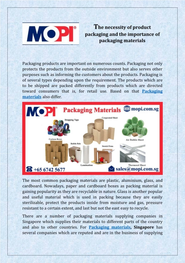
Download

1 / 4
50 likes | 94 Vues
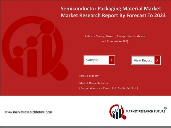
Semiconductor Packaging Materials Market

E N D
Summary Global Semiconductor Packaging Materials Market: By Type (Organic Substrates, Bonding Wires, Encapsulation Resins, Ceramic Packages, Solder Balls, Wafer Level Packaging Dielectrics and Others), Technology (Grid Array, Small Outline Package, Dual Flat No-Leads, Quad Flat Package, Dual In-Line Package And Others), And Region - Global Forecast To 2023 Semiconductor Packaging Materials Market Scenario Semiconductor Packaging Materials are useful during the final stage of semiconductor device fabrication. They are used for safeguarding devices from deterioration and external influence. Market Research Future (MRFR) has published a research report about the global Semiconductor Packaging Materials market that reckons proliferation for this market at 5% CAGR (Compound Annual Growth Rate) between 2017 and 2023. The acute factor for the global Semiconductor Packaging Materials market is increasing miniaturization of the electronic devices. Other important factors aiding the market growth include continuously growing mobile industry, increased demand for mobile & communication devices, increasing implementation of integrated circuits in various electronic devices, rapid technological advancements, shifting of the customer towards modern electronics, and lastly, increasing demand for compact devices across various sectors. Get Free Sample @ https://www.marketresearchfuture.com/sample_request/1217 Key Players The key players in the global Semiconductor Packaging Materials Market are •Henkel AG & Company •KGaA (Germany) •Hitachi Chemical Company, Ltd. (Japan) •Sumitomo Chemical Co., Ltd. (Japan) •Kyocera Chemical Corporation (Japan) •Mitsui High-tec, Inc. (Japan) •Toray Industries, Inc. (Japan) •Alent plc (U.K.) •LG Chem (South Korea) •BASF SE (Germany) •Tanaka Kikinzoku Group (Japan) •E. I. du Pont de Nemours and Company (U.S.) •Honeywell International Inc. (U.S.) •Toppan Printing Co., Ltd. (Japan) •Nippon Micrometal Corporation (Japan) •Alpha Advanced Materials (U.S.) Latest Industry News
Rigaku Europe SE and Fraunhofer IISB in have forged a strategic partnership to revolutionize the characterization of semiconductor materials by X-ray topography. Rigaku has installed the latest generation X-ray topography tool, the Rigaku XRTmicron imaging system, at Fraunhofer IISB. This topography tool offers insights into semiconductor material quality that includes packaging material too. 21 JAN 2019 Kulicke and Soffa Industries Inc., a leading provider of semiconductor packaging and electronic assembly solutions, has increased its three-year share repurchase program, by an additional US $ 100 mn. 31 JAN 2019 Regional Analysis The regional segmentation of the global Semiconductor Packaging Materials Market segments the market into the regional markets namely Europe, North America, Asia Pacific, and the Middle East & Africa (MEA). The Asia Pacific currently holds the highest position in the Semiconductor Packaging Materials market, and during the forecast period, the market is likely to rise further due to fast technological advancement and the developing demand for progressive electronic packaging materials from the end-users. At the same time, the large investments in electronics applications, easy convenience of the raw materials, low- cost manufacturing, and low workforce cost are pushing the market growth in this region. The prominent country-specific markets in this region are Australia, China, India, Japan, and South Korea, followed by the remaining countries of the Asia Pacific region. North America is another important regional market due to technological advancement, various established industries, and the presence of many key market players. The pivotal country-specific markets in this region are USA and Canada. Europe is another crucial regional market that is growing due to the reasons same as in North America. The significant country-specific markets in this region are France, Germany, Spain, and the UK, followed by the remaining countries of Europe. The MEA region is a small regional market due to poor countries, lack of awareness, lack of education, lack of infrastructure, and lack of technological advancement. Market Segmentation The global Semiconductor Packaging Materials market has been segmented on the basis of technology, type, and lastly, region. The technology-based segmentation segments the market into the dual in-line package, dual flat no-leads, grid array, quad flat package, small outline package, and others. During the forecast period, grid array is projected to be the fastest-growing technology due to its wide application across all major semiconductor packaging type. By type, the market has been segmented into bonding wires, ceramic packages, encapsulation resins, organic substrates, solder balls, wafer level packaging dielectrics, and others. During the forecast period, the organic substrates are expected to dominate the market due to their ability to form the base layers of single semiconductor devices and chips on which additional layers can be dumped to complete the circuit. Table Of Contents 1 Executive Summary
2 Scope Of The Report 2.1 Market Definition 2.2 Scope Of The Study 2.2.1 Definition 2.2.2 Research Objective 2.2.3 Assumptions 2.2.4 Limitations 2.3 Research Type 2.3.1 Primary Research 2.3.2 Secondary Research 2.4 Market Size Estimation 2.5 Forecast Model 3 Market Landscape 3.1 Porter’s Five Forces Analysis 3.1.1 Threat Of New Entrants 3.1.2 Bargaining Power Of Buyers 3.1.3 Threat Of Substitutes 3.1.4 Segment Rivalry 3.1.5 Bargaining Power Of Buyers 3.2 Value Chain/Supply Chain Analysis Continues….. List Of Figures FIGURE 1 RESEARCH TYPEOF MRFR FIGURE 2 TOP DOWN & BOTTOM UP APPROACH FIGURE 3 Market Dynamics FIGURE 4 Impact Analysis: Market Drivers FIGURE 5 Impact Analysis: Market Restraints FIGURE 6 Porter’s Five Forces Analysis FIGURE 7 Value Chain Analysis Continues……
Browse Full Report With Table Of Content @ https://www.marketresearchfuture.com/reports/semiconductor-packaging-material- market-1217 About Market Research Future At Market Research Future (MRFR), we enable our customers to unravel the complexity of various industries through our Cooked Research Report (CRR), Half-Cooked Research Reports (HCRR), Raw Research Reports (3R), Continuous-Feed Research (CFR), and Market Research & Consulting Services. MRFR team have supreme objective to provide the optimum quality market research and intelligence services to our clients. Our market research studies by products, services, technologies, applications, end users, and market players for global, regional, and country level market segments, enable our clients to see more, know more, and do more, which help to answer all their most important questions. In order to stay updated with technology and work process of the industry, MRFR often plans & conducts meet with the industry experts and industrial visits for its research analyst members. Contact Market Research Future Phone: +1646 845 9312 Email: sales@marketresearchfuture.com