Multicycle Datapath
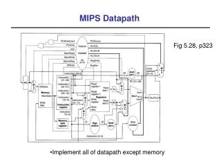
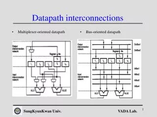
Enhance single-cycle datapath by reusing functional units, reduce extra hardware, and optimize instruction execution flow in a multicycle design. Implement stages for instruction fetch, execution with ALU computation, data memory access, and register file operations. Improve control with mux selectors for ALU inputs and a unified memory for instructions and data storage. Utilize intermediate registers to preserve functional unit outputs for later stages.


Multicycle Datapath
E N D
Presentation Transcript
Multicycle Datapath • As an added bonus, we can eliminate some of the extra hardware from the single-cycle datapath. • We will restrict ourselves to using each functional unit once per cycle, just like before. • But since instructions require multiple cycles, we could reuse some units in a different cycle during the execution of a single instruction. • For example, we could use the same ALU: • to increment the PC (first clock cycle), and • for arithmetic operations (third clock cycle). • Proposed execution stages • Instruction fetch and PC increment • Reading sources from the register file • Performing an ALU computation • Reading or writing (data) memory • Storing data back to the register file
Two extra adders • Our original single-cycle datapath had an ALU and two adders. • The arithmetic-logic unit had two responsibilities. • Doing an operation on two registers for arithmetic instructions. • Adding a register to a sign-extended constant, to compute effective addresses for lw and sw instructions. • One of the extra adders incremented the PC by computing PC + 4. • The other adder computed branch targets, by adding a sign-extended, shifted offset to (PC + 4).
0 M u x 1 1 M u x 0 Shift left 2 PCSrc RegWrite MemToReg MemWrite I [25 - 21] Read address Instruction [31-0] Read register 1 Read data 1 PC Read address Read data I [20 - 16] Read register 2 Instruction memory Read data 2 Write address 0 M u x 1 0 M u x 1 Write register Data memory Write data Registers I [15 - 11] Write data MemRead ALUSrc RegDst Sign extend I [15 - 0] The extra single-cycle adders Add 4 Add ALU Zero Result ALUOp
Our new adder setup • We can eliminate both extra adders in a multicycle datapath, and instead use just one ALU, with multiplexers to select the proper inputs. • A 2-to-1 mux ALUSrcA sets the first ALU input to be the PC or a register. • A 4-to-1 mux ALUSrcB selects the second ALU input from among: • the register file (for arithmetic operations), • a constant 4 (to increment the PC), • a sign-extended constant (for effective addresses), and • a sign-extended and shifted constant (for branch targets). • This permits a single ALU to perform all of the necessary functions. • Arithmetic operations on two register operands. • Incrementing the PC. • Computing effective addresses for lw and sw. • Adding a sign-extended, shifted offset to (PC + 4) for branches.
PC IorD RegDst RegWrite Read register 1 Read data 1 Read register 2 Address Read data 2 0 M u x 1 0 M u x 1 0 M u x 1 Write register Memory Write data Registers Write data Mem Data MemToReg The multicycle adder setup highlighted PCWrite ALUSrcA MemRead 0 M u x 1 ALU Zero Result 0 1 2 3 4 ALUOp MemWrite ALUSrcB Sign extend Shift left 2
Eliminating a memory • Similarly, we can get by with one unified memory, which will store both program instructions and data. (a Princeton architecture) • This memory is used in both the instruction fetch and data access stages, and the address could come from either: • the PC register (when we’re fetching an instruction), or • the ALU output (for the effective address of a lw or sw). • We add another 2-to-1 mux, IorD, to decide whether the memory is being accessed for instructions or for data. • Proposed execution stages • Instruction fetch and PC increment • Reading sources from the register file • Performing an ALU computation • Reading or writing (data) memory • Storing data back to the register file
PCWrite Shift left 2 IorD MemRead ALUSrcA PC 0 M u x 1 RegDst RegWrite Read register 1 Read data 1 ALU Read register 2 Zero Address Read data 2 4 0 1 2 3 Result 0 M u x 1 0 M u x 1 0 M u x 1 Write register MemWrite Memory ALUOp Write data Registers Write data Mem Data ALUSrcB Sign extend MemToReg The new memory setup highlighted
Intermediate registers • Sometimes we need the output of a functional unit in a later clock cycle during the execution of one instruction. • The instruction word fetched in stage 1 determines the destination of the register write in stage 5. • The ALU result for an address computation in stage 3 is needed as the memory address for lw or sw in stage 4. • These outputs will have to be stored in intermediate registers for future use. Otherwise they would probably be lost by the next clock cycle. • The instruction read in stage 1 is saved in Instruction register. • Register file outputs from stage 2 are saved in registers A and B. • The ALU output will be stored in a register ALUOut. • Any data fetched from memory in stage 4 is kept in the Memory data register, also called MDR.
PCSource Shift left 2 ALUSrcA PC IorD RegDst IRWrite RegWrite A Read register 1 Read data 1 ALU B Read register 2 Zero Address Read data 2 [31-26] [25-21] [20-16] [15-11] [15-0] 0 1 2 3 Result 0 M u x 1 0 M u x 1 0 M u x 1 0 M u x 1 0 M u x 1 Write register Memory ALUOp Write data Registers Write data Mem Data Instruction register ALUSrcB Memory data register Sign extend MemToReg The final multicycle datapath PCWrite MemRead ALU Out 4 MemWrite
Register write control signals • We have to add a few more control signals to the datapath. • Since instructions now take a variable number of cycles to execute, we cannot update the PC on each cycle. • Instead, a PCWrite signal controls the loading of the PC. • The instruction register also has a write signal, IRWrite. We need to keep the instruction word for the duration of its execution, and must explicitly re-load the instruction register when needed. • The other intermediate registers, MDR, A, B and ALUOut, will store data for only one clock cycle at most, and do not need write control signals.
Summary of Multicycle Datapath • A single-cycle CPU has two main disadvantages. • The cycle time is limited by the worst case latency. • It requires more hardware than necessary. • A multicycle processor splits instruction execution into several stages. • Instructions only execute as many stages as required. • Each stage is relatively simple, so the clock cycle time is reduced. • Functional units can be reused on different cycles. • We made several modifications to the single-cycle datapath. • The two extra adders and one memory were removed. • Multiplexers were inserted so the ALU and memory can be used for different purposes in different execution stages. • New registers are needed to store intermediate results. • Next time, we’ll look at controlling this datapath.
PCWrite Shift left 2 PC ALUSrcA ALU Out IorD RegDst RegWrite [31-26] [25-21] [20-16] [15-11] [15-0] MemRead Read register 1 Read data 1 ALU Read register 2 Zero Read data 2 Address Instruction register 0 1 2 3 IRWrite Result 0 M u x 1 0 M u x 1 0 M u x 1 0 M u x 1 0 M u x 1 Write register Memory ALUOp 4 Memory data register A PCSource Write data Registers Write data Mem Data B MemWrite Sign extend ALUSrcB MemToReg Controlling the multicycle datapath • Now we talk about how to control this datapath.
Multicycle control unit • The control unit is responsible for producing all of the control signals. • Each instruction requires a sequence of control signals, generated over multiple clock cycles. • This implies that we need a state machine. • The datapath control signals will be outputs of the state machine. • Different instructions require different sequences of steps. • This implies the instruction word is an input to the state machine. • The next state depends upon the exact instruction being executed. • After we finish executing one instruction, we’ll have to repeat the entire process again to execute the next instruction.
R-type execution R-type writeback Op = R-type Instruction fetch and PC increment Branch completion Register fetch and branch computation Op = BEQ Memory write Effective address computation Op = SW Memory read Register write Op = LW/SW Op = LW Finite-state machine for the control unit • Each bubble is a state • Holds the control signals for a single cycle • Note: All instructions do the same things during the first two cycles
Stage 1: Instruction Fetch • Stage 1 includes two actions which use two separate functional units: the memory and the ALU. • Fetch the instruction from memory and store it in IR. IR = Mem[PC] • Use the ALU to increment the PC by 4. PC = PC + 4
PCWrite Shift left 2 PC ALUSrcA ALU Out IorD RegDst RegWrite [31-26] [25-21] [20-16] [15-11] [15-0] MemRead Read register 1 Read data 1 ALU Read register 2 Zero Address Read data 2 Instruction register 0 1 2 3 IRWrite Result 0 M u x 1 0 M u x 1 0 M u x 1 0 M u x 1 0 M u x 1 Write register Memory ALUOp 4 Memory data register A PCSource Write data Registers Write data Mem Data B MemWrite Sign extend ALUSrcB MemToReg Stage 1: Instruction Fetch
Stage 2: Read registers • Stage 2 is much simpler. • Read the contents of source registers rs and rt, and store them in the intermediate registers A and B. (Remember the rs and rt fields come from the instruction register IR.) A = Reg[IR[25-21]] B = Reg[IR[20-16]]
PCWrite Shift left 2 PC ALUSrcA ALU Out IorD RegDst RegWrite [31-26] [25-21] [20-16] [15-11] [15-0] MemRead Read register 1 Read data 1 ALU Read register 2 Zero Address Read data 2 Instruction register 0 1 2 3 IRWrite Result 0 M u x 1 0 M u x 1 0 M u x 1 0 M u x 1 0 M u x 1 Write register Memory ALUOp 4 Memory data register A PCSource Write data Registers Write data Mem Data B MemWrite Sign extend ALUSrcB MemToReg Stage 2: Register File Read
Stage 2 control signals • No control signals need to be set for the register reading operations A = Reg[IR[25-21]] and B = Reg[IR[20-16]]. • IR[25-21] and IR[20-16] are already applied to the register file. • Registers A and B are already written on every clock cycle.
Executing Arithmetic Instructions: Stages 3 & 4 • We’ll start with R-type instructions like add $t1, $t1, $t2. • Stage 3 for an arithmetic instruction is simply ALU computation. ALUOut = A op B • A and B are the intermediate registers holding the source operands. • The ALU operation is determined by the instruction’s “func” field and could be one of add, sub, and, or, slt. • Stage 4, the final R-type stage, is to store the ALU result generated in the previous cycle into the destination register rd. Reg[IR[15-11]] = ALUOut
PCWrite Shift left 2 PC ALUSrcA ALU Out IorD RegDst RegWrite [31-26] [25-21] [20-16] [15-11] [15-0] MemRead Read register 1 Read data 1 ALU Read register 2 Zero Address Read data 2 Instruction register 0 1 2 3 IRWrite Result 0 M u x 1 0 M u x 1 0 M u x 1 0 M u x 1 0 M u x 1 Write register Memory ALUOp 4 Memory data register A PCSource Write data Registers Write data Mem Data B MemWrite Sign extend ALUSrcB MemToReg Stage 3 (R-Type): ALU operation
PCWrite Shift left 2 PC ALUSrcA ALU Out IorD RegDst RegWrite [31-26] [25-21] [20-16] [15-11] [15-0] MemRead Read register 1 Read data 1 ALU Read register 2 Zero Address Read data 2 Instruction register 0 1 2 3 IRWrite Result 0 M u x 1 0 M u x 1 0 M u x 1 0 M u x 1 0 M u x 1 Write register Memory ALUOp 4 Memory data register A PCSource Write data Registers Write data Mem Data B MemWrite Sign extend ALUSrcB MemToReg Stage 4 (R-Type): Register Writeback
Executing a beq instruction • We can execute a branch instruction in three stages or clock cycles. • But it requires a little cleverness… • Stage 1 involves instruction fetch and PC increment. IR = Mem[PC] PC = PC + 4 • Stage 2 is register fetch and branch target computation. A = Reg[IR[25-21]] B = Reg[IR[20-16]] • Stage 3 is the final cycle needed for executing a branch instruction. • Assuming we have the branch target available if (A == B) then PC = branch_target
When should we compute the branch target? • We need the ALU to do the computation. • When is the ALU not busy?
Optimistic execution • But, we don’t know whether or not the branch is taken in cycle 2!! • That’s okay…. we can still go ahead and compute the branch target first. The book calls this optimistic execution. • The ALU is otherwise free during this clock cycle. • Nothing is harmed by doing the computation early. If the branch is not taken, we can just ignore the ALU result. • This idea is also used in more advanced CPU design techniques. • Modern CPUs perform branch prediction, which we’ll discuss in a few lectures in the context of pipelining.
Stage 2 Revisited: Compute the branch target • To Stage 2, we’ll add the computation of the branch target. • Compute the branch target address by adding the new PC (the original PC + 4) to the sign-extended, shifted constant from IR. ALUOut = PC + (sign-extend(IR[15-0]) << 2) We save the target address in ALUOut for now, since we don’t know yet if the branch should be taken. • What about R-type instructions that always go to PC+4 ?
PCWrite Shift left 2 PC ALUSrcA ALU Out IorD RegDst RegWrite [31-26] [25-21] [20-16] [15-11] [15-0] MemRead Read register 1 Read data 1 ALU Read register 2 Zero Address Read data 2 Instruction register 0 1 2 3 IRWrite Result 0 M u x 1 0 M u x 1 0 M u x 1 0 M u x 1 0 M u x 1 Write register Memory ALUOp 4 Memory data register A PCSource Write data Registers Write data Mem Data B MemWrite Sign extend ALUSrcB MemToReg Stage 2 (Revisited): Branch Target Computation
Branch completion • Stage 3 is the final cycle needed for executing a branch instruction. if (A == B) then PC = ALUOut • Remember that A and B are compared by subtracting and testing for a result of 0, so we must use the ALU again in this stage.
PCWrite Shift left 2 PC ALUSrcA ALU Out IorD RegDst RegWrite [31-26] [25-21] [20-16] [15-11] [15-0] MemRead Read register 1 Read data 1 ALU Read register 2 Zero Address Read data 2 Instruction register 0 1 2 3 IRWrite Result 0 M u x 1 0 M u x 1 0 M u x 1 0 M u x 1 0 M u x 1 Write register Memory ALUOp 4 Memory data register A PCSource Write data Registers Write data Mem Data B MemWrite Sign extend ALUSrcB MemToReg Stage 3 (BEQ): Branch Completion
Executing a sw instruction • A store instruction, like sw $a0, 16($sp), also shares the same first two stages as the other instructions. • Stage 1: instruction fetch and PC increment. • Stage 2: register fetch and branch target computation. • Stage 3 computes the effective memory address using the ALU. ALUOut = A + sign-extend(IR[15-0]) A contains the base register (like $sp), and IR[15-0] is the 16-bit constant offset from the instruction word, which is not shifted. • Stage 4 saves the register contents (here, $a0) into memory. Mem[ALUOut] = B Remember that the second source register rt was already read in Stage 2 (and again in Stage 3), and its contents are in intermediate register B.
PCWrite Shift left 2 PC ALUSrcA ALU Out IorD RegDst RegWrite [31-26] [25-21] [20-16] [15-11] [15-0] MemRead Read register 1 Read data 1 ALU Read register 2 Zero Address Read data 2 Instruction register 0 1 2 3 IRWrite Result 0 M u x 1 0 M u x 1 0 M u x 1 0 M u x 1 0 M u x 1 Write register Memory ALUOp 4 Memory data register A PCSource Write data Registers Write data Mem Data B MemWrite Sign extend ALUSrcB MemToReg Stage 3 (SW): Effective Address Computation
PCWrite Shift left 2 PC ALUSrcA ALU Out IorD RegDst RegWrite [31-26] [25-21] [20-16] [15-11] [15-0] MemRead Read register 1 Read data 1 ALU Read register 2 Zero Address Read data 2 Instruction register 0 1 2 3 IRWrite Result 0 M u x 1 0 M u x 1 0 M u x 1 0 M u x 1 0 M u x 1 Write register Memory ALUOp 4 Memory data register A PCSource Write data Registers Write data Mem Data B MemWrite Sign extend ALUSrcB MemToReg Stage 4 (SW): Memory Write
Executing a lw instruction • Finally, lw is the most complex instruction, requiring five stages. • The first two are like all the other instructions. • Stage 1: instruction fetch and PC increment. • Stage 2: register fetch and branch target computation. • The third stage is the same as for sw, since we have to compute an effective memory address in both cases. • Stage 3: compute the effective memory address.
Stages 4-5 (lw): memory read and register write • Stage 4 is to read from the effective memory address, and to store the value in the intermediate register MDR (memory data register). MDR = Mem[ALUOut] • Stage 5 stores the contents of MDR into the destination register. Reg[IR[20-16]] = MDR Remember that the destination register for lw is field rt (bits 20-16) and not field rd (bits 15-11).
PCWrite Shift left 2 PC ALUSrcA ALU Out IorD RegDst RegWrite [31-26] [25-21] [20-16] [15-11] [15-0] MemRead Read register 1 Read data 1 ALU Read register 2 Zero Address Read data 2 Instruction register 0 1 2 3 IRWrite Result 0 M u x 1 0 M u x 1 0 M u x 1 0 M u x 1 0 M u x 1 Write register Memory ALUOp 4 Memory data register A PCSource Write data Registers Write data Mem Data B MemWrite Sign extend ALUSrcB MemToReg Stage 4 (LW): Memory Read
PCWrite Shift left 2 PC ALUSrcA ALU Out IorD RegDst RegWrite [31-26] [25-21] [20-16] [15-11] [15-0] MemRead Read register 1 Read data 1 ALU Read register 2 Zero Address Read data 2 Instruction register 0 1 2 3 IRWrite Result 0 M u x 1 0 M u x 1 0 M u x 1 0 M u x 1 0 M u x 1 Write register Memory ALUOp 4 Memory data register A PCSource Write data Registers Write data Mem Data B MemWrite Sign extend ALUSrcB MemToReg Stage 5 (LW): Register Writeback
ALUSrcA = 1 ALUSrcB = 00 ALUOp = 110 PCWrite = Zero PCSource = 1 RegWrite = 1 RegDst = 1 MemToReg = 0 ALUSrcA = 1 ALUSrcB = 00 ALUOp = func ALUSrcA = 0 ALUSrcB = 11 ALUOp = 010 IorD = 0 MemRead = 1 IRWrite = 1 ALUSrcA = 0 ALUSrcB = 01 ALUOp = 010 PCSource = 0 PCWrite = 1 MemWrite = 1 IorD = 1 ALUSrcA = 1 ALUSrcB = 10 ALUOp = 010 RegWrite = 1 RegDst = 0 MemToReg = 1 MemRead = 1 IorD = 1 Finite-state machine for the control unit R-type execution R-type writeback Op = R-type Instruction fetch and PC increment Branch completion Register fetch and branch computation Op = BEQ Memory write Effective address computation Op = SW Memory read Register write Op = LW/SW Op = LW
Implementing the FSM • This can be translated into a state table; here are the first two states. • You can implement this the hard way. • Represent the current state using flip-flops or a register. • Find equations for the next state and (control signal) outputs in terms of the current state and input (instruction word). • Or you can use the easy way. • Stick the whole state table into a memory, like a ROM. • This would be much easier, since you don’t have to derive equations.
Summary • Now you know how to build a multicycle controller! • Each instruction takes several cycles to execute. • Different instructions require different control signals and a different number of cycles. • We have to provide the control signals in the right sequence.