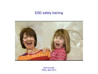
ESD safety training
ESD safety training. Donna Kubik FNAL, April 2014. But, static is not always fun!. It can lead to damage of sensitive semiconductor devices. Outline of ESD safety training. Slides on ESD safety Video about ESD safety. Static charge.

ESD safety training
E N D
Presentation Transcript
ESD safety training Donna Kubik FNAL, April 2014
But, static is not always fun! It can lead to damage of sensitive semiconductor devices
Outline of ESD safety training • Slides on ESD safety • Video about ESD safety
Static charge • Electrostatic electricity is an imbalance of positive and negative charges on the surface of objects. • For example, a person can generate static charge while walking across the floor. • The human body can charge to 100s or 1000s of volts. +500 V -
Static charge • For example, once charged, discharge from the finger tip to a CCD is possible, creating an electrostatic discharge (ESD) event. • The tiniest spark requires about 500 V, which more than 10 times more than a typical CCD gate dielectric can withstand before damage results. +500 V-
Triboelectric effect • How does the imbalance of charge get created? • One very common way is to rub two objects together. • If they are made of different materials and are both insulators electrons may be transferred from one to the other. • The more rubbing, the more electrons move, and the larger the static charge that builds up. • This is called the triboelectric effect • Tribo- means ‘to rub’.
Triboelectric effect • Note: It is not the rubbing or friction that causes electrons to move. • It is simply the contact between two different materials. • Rubbing just increases the contact area between them.
Triboelectric series • When we rub two different materials together, which becomes positively charged and which becomes negative? • Materials have been ranked according to their ability to hold or give up electrons. • This ranking is called the triboelectric series. • When 2 materials are rubbed together, the one higher on the list will give up electrons and become positively charged.
Why does your hair stand up after you put on a wool sweater? • When you put on your sweater, it rubs against your hair. • Electrons move from your hair to the sweater. (Hair is above wool on the tribolectric series) • Now each of the hairs has the same positive charge. • Things with the same charge repel each other. • So the hairs try to move away from each other. • The farthest apart they can get is to stand up and away from all the other hairs.
Does this happen to bees, too? • As they travel through the air, bees lose electrons, accumulating a small positive electrical charge. • Flowers have a natural negative electric charge and conduct electrons from the air to the ground. • As a bee approaches a flower, a tiny electric field is created between plant and bee. • A new study showed that the bee’s landing actually changes the flower’s electrical charge for a short period of time. • The study's authors hypothesize that this change may signal to the next bee that the flower has just been visited and that its nectar is depleted. Science, 2013. DOI: 10.1126/science.1230883
Static charge and bees • It’s unclear exactly how bees can sense these electrical fields, but it’s possible that their tiny hairs can bristle up when exposed to positive charges, just as our hair stands on end in response to static electricity. Science, 2013. DOI: 10.1126/science.1230883
Static charge and CCDs • The CCD is one of the most ESD-sensitive electronic components manufactured. • Without ESD protection diodes, most scientific CCDs are susceptible to damage by electrostatic discharge. • An ESD event can cause bus lines to melt, generate ESD craters, diode junction breakdown, or insulator failure. • “Of these problems, dielectric damage is by far most prevalent.”* *Scientific CCDs, J. R. Janesick
Static charge and CCDs • Although any semiconductor device can be damaged by a spark, MOS (Metal Oxide Semiconductor) devices are particularly susceptible. • This is because the energy stored in the gate-channel capacitance, when it has been brought up to breakdown voltage, is sufficient to blow a hole through the delicate gate oxide insulation.* • The gate oxide insulation is the dielectric mentioned in the previous slide. Gate oxide damage to an input buffer *The Art of Electronics, Horowitz and Hill
The need to practice ESD-safe procedures • ESD gate protection helps, but it is not perfect (described in Appendix) • The most vulnerable (small) gates do get useful protection. • But very fast ESD spikes can still get through, and transistor drains are not protected. • The CCDs used at Sidet have no on-chip ESD protection • DECam • DAMIC • CONNIE • MS_DESI • Therefore, there is no substitute for careful procedure.
The need to practice ESD-safe procedures • Internal ESD protection networks of resistors and clamping diodes can • compromise performance • speed, noise • complicate device design • cause luminescence An example of amplifier luminescence can be seen in the upper left hand corner of this image. Luminescence could also be caused by a conducting diode.
Front-illuminated vs. back-illuminated CCDs • For bare wafers or front-illuminated chips it is sometimes possible to view ESD damage under a microscope. • However, DECam CCDs (and most research-grade CCDs) are back-illuminated, so, once packaged, it is not possible to see the damage. • Fault analysis is harder or impossible.
The need to practice ESD-safe procedures • There is also a concern about non-fatal ESD damage. • This could manifest itself as delayed failure or performance degradation, both of which are bad news. • Again, there is no substitute for careful procedure.
The need to practice ESD-safe procedures • Therefore, at Fermilab, ASIC designers often rely on the skill and care of the technicians to practice ESD safe procedures when packaging, installing, and testing devices rather than sacrificing performance or complicating the design by including internal protection.* *Jim Hoff, Fermilab ASIC Designer
Laser diodes • Laser diodes are ESD-sensitive • At Sidet • Used in SPDC experiment • CCD characterization
Laser diode failure mechanisms* • Over-voltage or over-current condition. • Electrical overstress: Failure of a laser diode’s P-N junction itself. A severe over-current or over-voltage power surge can cause localized heating and other harmful phenomena, which, under extreme conditions, can actually fracture the laser diode die. • Low-power laser diodes, that is, laser diodes whose optical output power is below around 200 mW, are particularly sensitive to ESD. • This is because they are designed to be inherently fast devices. Low-power laser diodes are often directly modulated and used for fiber-optic communication with data rates in the gigahertz range. • Thus the P-N junction and optical elements of a laser diode can react very quickly to changes in voltage or current. *Source: http://www.lasorb.com/04_damage-mechanisms.htm
Transistors • Especially the newer InP-based High Electron Mobility Transistors(HEMTs) • QUIET • MKIDs • Devices will typically start degrading with drain to gate voltage exceeding 2.5 V. • Protect the drain at +1.8V and -.6 V and the gate at +- .6 V. • There are typically two reasons for much lower breakdown than in either GaAs or Si devices. • Low Schottky barrier height for AlInAs • Lower avalanche breakdown in InGaAs .
3D technology at Fermilab • Stacking several silicon wafers and interconnecting them vertically with TSV (through-silicon vias) enables the creation of truly three-dimensional devices. • Challenging ESD problems “antenna effects” • Each layer needs an “antenna diode” to protect the devices during the assembly process. • Need to test at intermediate steps.
Adiabatic Demagnetization Refrigerator (ADR) • Always wear a wrist strap when working on or near the ADR, when the cryostat is both open and closed. • In addition to sensitive devices that are part of the test setup, the heat switch controls are ESD-sensitive. heat switch control box wrist strap ADR cryostat open ADR cryostat closed
ADR heat switch Close-up view of ADR heat switch control box ADR heat swtich
CMS • Sensors tend to be rather insensitive to ESD because of the thick oxides and large capacitance. • But the ICs are quite sensitive.
ESD-sensitive CMS electronics • The ROC is most sensitive. • Must also be careful handling the HDI, for it’s connected to the ROC.
CMS Pixel Specific Information • Design of CMS pixel detector sensors and electronics very similar to that of original detector. • Based on past experience, we do not expect to lose modules / sensors / electronics due to ESD if proper handling rules are followed. • However we have recently damaged readout chips due to improper handling. • Still have to understand exact mechanism that causes the damage and which parts are most sensitive to ESD. • Expect readout chips to be more sensitive to ESD than sensors. CMS Pixel Specific Information
When can damage happen? • Handling of wafers (sensors, readout chips and ancillary electronics) • Handling of individual electronics parts (HDIs populated with discrete components and TBM, individual readout chips) • Handling of modules (sensor + readout chips + HDI) • Some assembly steps done in industry, some at universities and Fermilab CMS Pixel Specific Information
Minimizing damage risk • Risks • Placing wafers on probe stations at multiple sites • Placing sensors and HDIs on gantry system at Purdue and Nebraska • Placing HDIs on probe stations for testing • Placing assembled modules on carrier boards • Connecting modules to test boards • Installing modules on half disks • Shipping / transporting / storing parts • Handling of individual chips • In some cases we try to minimize risks by using protective covers. Even in these cases you have to be properly connected to ground. CMS Pixel Specific Information
Other protective measures • Parts stored in cabinets flushed with dry air • Cabinets are grounded • Static dissipative mats on the shelves • Flush dry air in cold boxes during testing (and monitor humidity and temperature) CMS Pixel Specific Information
Humidity helps • If it is very humid, the charge imbalance will not remain for long time. • If the humidity is high, the moisture coats the surface of the material, providing a low-resistance path for electron flow. • This path allows the charges to "recombine" and thus neutralize the charge imbalance. • If it is very dry, a charge can build up to extraordinary levels, up to tens of thousands of volts!
Humidity Humidity and temperature are monitored and recorded 24/7 in all cleanrooms at Sidet. The alarm will sound if the relative humidity gets below 35%. If the alarm sounds, it can be silenced, but you should stop ESD-sensitive work until the humidity level is restored. Humidity and temperature monitor Humidity and temperature monitor in C100 cleanroom
Humidity is not enough • As the table shows, triboelectric charging persists, even at high relative humidity. • Humidity control does limit the triboelectric charging process, buthumidity does not eliminate the need for all of the conventional safeguards!
The need to practice ESD-safe procedures • There is no substitute for careful procedure. • Therefore we must follow all ESD safety procedures very carefully to minimize the chance of damaging the CCDs: • Constant monitoring of grounding • ESD-safe garments • ESD-safe workspace
Continuous ESD monitoring Wrist strap ionizer CCD test dewar Remote module Ground Gard 5 SPI-94391 MAT GND Wrist strap Wrist strap Power AC power Floor mat
Types of continuous wrist strap monitors • There are several systems of continuous wrist strap monitors. • The most common are • Single conductor monitors • Dual conductor monitors
Single conductor continuous wrist strap monitors • The wrist strap monitors we currently use fin most areas are single conductor monitors • A person can be thought of as a plate of a capacitor with the other plate being ground. • The “plates” are separated by an insulator as shoes and mats. • The person and the resistors built into the wrist strap and connecting cords form the resistor.
Single conductor continuous wrist strap monitors • A 30 mVAC current applied to this circuit provides a way to measure whether the circuit is complete. • Any break will cause a higher impedance that can be used to trigger an audible alarm.
Dual conductor continuous wrist strap monitors • A tiny pulsed DC current applied to this circuit provides a way to measure whether the circuit is complete. • The voltage at your wrist is < 300 mVDC. • Any break will trigger an audible alarm.
Ionizer bar ionizer bar located under hood + - + - + - + - + - + - + - + - + - + - + - + - + - + - + -