Processing Units: Basic Cycle and Control Mechanisms
Learn about the basic processing cycle, types of operations, control mechanisms, and register transfers in the processing unit of a computer. Explore examples of arithmetic/logic operations and branching operations.

Processing Units: Basic Cycle and Control Mechanisms
E N D
Presentation Transcript
Basic Processing Unit(Chapter 7) http://www.pds.ewi.tudelft.nl/~iosup/Courses/2011_ti1400_6.ppt Course website: http://www.pds.ewi.tudelft.nl/~iosup/Courses/2012_ti1400_results.htm
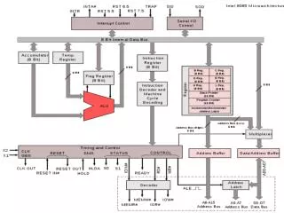
Problem instruction ? y Decoder f ALU a y Reg
X: 1 Y: 2 Z: 3 • • READ(X) READ(Y) ADD(X,Y,Z) WRITE(Z) Lecture 2Von Neumann Architecture Memory (Central) Processing Unit TEMP_A: TEMP_B: RESULT: arithmetic unit Input IR: CONTROL Output PC:
The Processing Unit Basic Processing Cycle Types of Operations Control Mechanisms 4
Basic Processing Cycle • Assume an instruction occupies a 32 bit single word in byte addressable memory • Basic cycleto be implemented: 1. Fetch instruction pointed to by PC and put it into the Instruction Register (IR): [IR] M([PC]) 2. Increment PC:[PC] [PC] + 4 3. Perform actions as specified in IR
Organization CPU bus Decoder PC control MAR IR memory bus MDR Register file R0 Y R1 R2 ALU Rn-1 Z
MUX Register gating CPU bus Y_in Const 4 Ri_in x Y x Ri Select x ALU Z_in x Ri_out Z x Z_out
R/W R/W R/W C C C D D D Q Q Q Edge-triggered D flip-flop Register gating Multiplexer R1_in R2_in R3_in 1 0 I I I C C C R1_out R2_out R3_out 1 bit of common bus line Tri-state gate: high impedance iff Ri_out=0, Q iff Ri_out=1
Multiple Datapaths Bus A R0 Y R1 R2 R3 ALU register file Bus B Bus C
The Processing Unit Basic Processing Cycle Types of Operations Control Mechanisms Register Transfer Fetch from Memory Store to Memory Arithmetic/Logic Ops. Complete Example Branching Ops. 10
2. Types of Operations • Operation cycle includes: • Transfer datafrom register to register or to ALU • Fetchcontents of memory location and put in one of the CPU registers • Storecontents of CPU register in memory location • Perform arithmetic or logic operation
2.1. Register Transfers R_out CPU bus Copy contents of R1 to R3 1.Address_out=R1 2. R_out 3. Address_in=R3 4. R_in R0 Y R1 R2 ALU R3 Z register file 1. R1_out 2. R3_in Address_out R_in Address_in
2.2. Fetch from Memory (1) Memory bus Data lines Internal processor bus MDR_outE MDR_out x x MDR x x MDR_in MDR_inE
2.2. Fetch from memory (2) e.g., Move (Ri),Rj Control Step 1 1. MAR [Ri] 2. Start read on memory bus 3. Wait for MFC response 4. Load MDR from memory bus 5. Rj [MDR] Memory Function Complete Control Step 2 Control Step 3 Address MAR Data MDR CPU Read Memory MFC
Signal Activation Sequence Fetch from memory (3) Internal processor bus Control Step 1. Ri_out, MAR_in, Read Control Step 2. MDR_inE, WMFC Control Step 3. MDR_out, Rj_in Ri_in x MDR_outE MDR_out Ri x x Memory bus Data lines MDR x x x Ri_out MDR_in MDR_inE
2.2. Fetch from Memory (4) Timing of the Operation 1 2 3 CLK 1. Ri_out, MAR_in, Read 2. MDR_inE, WMFC 3. MDR_out, Rj_in MAR_in address MAR to Mem.Bus New Address Read MR Mem.Read Cmd. MDR_inE Data Mem.Bus to MDR Value MFC Mem.Fnc.Complete MDR_out
2.3. Store to Memory e.g., Move Rj,(Ri) 1. Ri_out, MAR_in 2. Rj_out, MDR_in, Write 3. MDR_outE, WMFC Address Data Memory CPU Write MFC
2.4. Arithmetic Operation ADD R3,R2,R1 Step Action 1. Address_out R1 Y_in R_out 2. Address_out R2 R_out F_alu “ADD” Z_in Address_in R3 Z_out R_in
1. Address_out R1 Y_in R_out Register Transfers R_out CPU bus R0 Y_in Y R1 R2 ALU R3 Z register file Address_out
Arithmetic Operation ADD R3,R2,R1 Step Action 1. Address_out R1 Y_in R_out 2. Address_out R2 R_out F_alu “ADD” Z_in Address_in R3 Z_out R_in
2. Address_out R2 R_out F_alu “ADD” Z_in Register Transfers CPU bus R_out R0 Y_in Y R1 R2 F_alu ALU R3 Z_in Z register file Address_out
Arithmetic Operation ADD R3,R2,R1 Step Action 1. Address_out R1 Y_in R_out 2. Address_out R2 R_out F_alu “ADD” Z_in Address_in R3 Z_out R_in
Address_in R3 Z_out R_in Register Transfers CPU bus R0 Y R1 R2 ALU R3 Z register file R_in Z_out Address_in
Steps in time CPU bus Step 1 2 3 Y_in Y Y_in ALU Z_in Z_in Z Z_out R_in Z_out
The Processing Unit Basic Processing Cycle Types of Operations Control Mechanisms Register Transfer Fetch from Memory Store to Memory Arithmetic/Logic Ops. Complete Example Branching Ops. 26
2.5. Execution of a Complete Instruction 1. Fetch instruction 2. Fetch the operand 3. Perform operation 4. Store result • Example ADD (R3),R1 [R1] M([R3]) + [R1]
Execution fetch (1) Step 1-3: Instruction fetch and PC update Step Action 1 PC_out, MAR_in, Read Set carry-in ALU F_alu = “ADD” Z_in Z_out, PC_in Wait for MFC 3 MDR_out, IR_in [PC][PC ]+1 [IR]M([PC ]) Note: for architectures having PC:=PC+4 a different scheme must be used
1. PC_out, MAR_in, Read Set carry-in ALU F_alu = “ADD” Z_in Fetch instruction Q Why MAR_in? MAR_in MAR PC_out IR PC ADD ALU MDR carry Z_in Z Read WFMC Q Why Set carry-in ALU?
Execution fetch (2) Step 1-3: instruction fetch and PC update Step Action 1 PC_out, MAR_in, Read Set carry-in ALU F_alu = “ADD” Z_in Z_out, PC_in Wait for MFC 3 MDR_out, IR_in [PC][PC ]+1 [IR]M([PC ])
. Z_out, PC_in Wait for MFC Fetch instruction MAR_in MAR PC_in IR PC ALU MDR MDR_in Z Read Z_out Q What is read into MDR? WFMC
Execution fetch (3) Step 1-3: instruction fetch and PC update Step Action 1 PC_out, MAR_in, Read Set carry-in ALU F_alu = “ADD” Z_in Z_out, PC_in Wait for MFC 3 MDR_out, IR_in [PC ] [PC ]+1 [IR] M([PC ])
3. MDR_out, IR_in Fetch instruction Q What is loaded into IR? MAR IR PC IR_in ALU MDR Z Read MDR_out WFMC
Execute Step Action 4 Address_out=R3, R_out MAR_in Read Address_out=R1, R_out Y_in, Wait for MFC 6 MDR_out, Z_in F_alu = “ADD” 7 Address_in=R1, R_in Z_out, End Step 4 and 5: operand fetch Perform addition Store Result
Q Role of Decoder? 4. R3_out MAR_in Read Execute CPU bus Read PC Decoder control MAR IR memory bus MDR register file R0 Y R1 R2 ALU R3 Z
Execute Step Action 4 Address_out=R3, R_out MAR_in Read Address_out=R1, R_out Y_in, Wait for MFC 6 MDR_out, Z_in F_alu = “ADD” 7 Address_in=R1, R_in Z_out, End Step 4 and 5: operand fetch Perform addition Store Result
Q Where does MDRread from? . R1_out Y_in, Wait for MFC Execute CPU bus Decoder WFMC PC control MAR IR memory bus MDR R0 Y R1 R2 ALU R3 Z register file
Execute Step Action 4 Address_out=R3, R_out MAR_in Read Address_out=R1, R_out Y_in, Wait for MFC 6 MDR_out, Z_in F_alu = “ADD” 7 Address_in=R1, R_in Z_out, End Step 4 and 5: operand fetch Perform addition Store Result
Q Who sets F_alu to ADD? 6. MDR_out, Z_in F_alu = “ADD” Execute CPU bus Decoder PC control MAR IR memory bus MDR register file R0 Y R1 R2 ALU Q Why Z_in? R3 Z
Execute Step Action 4 Address_out=R3, R_out MAR_in Read Address_out=R1, R_out Y_in, Wait for MFC 6 MDR_out, Z_in F_alu = “ADD” 7 Address_in=R1, R_in Z_out, End Step 4 and 5: operand fetch Perform addition Store Result
Q Role of End? 7. R1_in Z_out, End Execute CPU bus Decoder PC control MAR IR memory bus MDR register file R0 Y R1 R2 ALU R3 Z
The Processing Unit Basic Processing Cycle Types of Operations Control Mechanisms Register Transfer Fetch from Memory Store to Memory Arithmetic/Logic Ops. Complete Example Branching Ops. 42
2.6. Branching Jump PC+Offset Step Action 1-3 <instruction fetch as in previous example> PC_out, Y_in 5 Offset-field-IR_out F_alu = “ADD” Z_in 6 PC_in Z_out, End
. PC_out, Y_in Branching CPU bus Decoder PC control MAR IR memory bus MDR register file R0 Y R1 R2 ALU R3 Z
Branching Step Action 1-3 <instruction fetch as in previous example> PC_out, Y_in 5 Offset-field-IR_out F_alu = “ADD” Z_in 6 PC_in Z_out, End
5. Offset-field-IR_out F_alu = “ADD” Z_in Branching CPU bus Decoder PC control MAR IR memory bus MDR register file R0 Y R1 R2 ALU R3 Z
Branching Step Action 1-3 <instruction fetch as in previous example> PC_out, Y_in 5 Offset-field-IR_out F_alu = “ADD” Z_in 6 PC_in Z_out, End
6. PC_in Z_out, End Branching CPU bus Decoder PC control MAR IR memory bus MDR R0 Y R1 R2 ALU R3 Z register file
Conditional branching JN PC+Offset Step Action 1-3 <instruction fetch as in previous example> PC_out, Y_in If N=0 then End 5 Offset-field-IR_out F_alu = “ADD” Z_in 6 PC_in Z_out, End If not Negative
The Processing Unit Basic Processing Cycle Types of Operations Control Mechanisms Hardwired Micro-Programmed Q Who sets F_alu to ADD? 50
3. Control Mechanisms • There are two basic control organizations: • Hardwired control • Micro-programmed control