Download
1 / 17
170 likes | 323 Vues
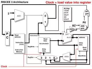
RISCEE 3 Architecture. Clock = load value into register. ALUop 1 X+0 2 X-Y 3 0+Y 4 0 5 X+Y. OR gate. 2. 0 1. ADD1. P0. BZ. AND gate. NOT. PC. Y. Zero. Read address Instruction [15-0] Instruction Memory. Instruction[7-0]. ALU3. address Write Data Read Data.

E N D
RISCEE 3 Architecture Clock = load value into register ALUop1 X+02 X-Y3 0+Y4 05 X+Y OR gate 2 0 1 ADD1 P0 BZ AND gate NOT PC Y Zero Readaddress Instruction[15-0] InstructionMemory Instruction[7-0] ALU3 address WriteData ReadData Read Data Accumulator WriteData X RegWrite MemWrite ADD2 3 2 1 0 RegDst Clock
Instruction: clear Operation: A=0; ALUop1 X+02 X-Y3 0+Y4 05 X+Y OR gate 2 0 1 ADD1 =0 P0 =0 BZ AND gate NOT PC Y Zero Readaddress Instruction[15-0] InstructionMemory Instruction[7-0] ALU3 address WriteData ReadData Read Data Accumulator WriteData X RegWrite =1 MemWrite RISCEE 3 Architecture ADD2 3 2 1 0 RegDst =0 =2 RegDst=2 ALU=4 MemWrite=0 RegWrite=1 BZ=0 P0=0
Instruction: addi data8 Operation: A = A + data8; ALUop1 X+02 X-Y3 0+Y4 05 X+Y OR gate 2 0 1 ADD1 =0 P0 =0 BZ AND gate NOT PC Y Zero Readaddress Instruction[15-0] InstructionMemory Instruction[7-0] ALU3 address WriteData ReadData Read Data Accumulator WriteData X RegWrite =1 MemWrite RISCEE 3 Architecture ADD2 3 2 1 0 RegDst =0 =2 RegDst=2 ALU=5 MemWrite=0 RegWrite=1 BZ=0 P0=0
Instruction: add addr8 Operation: A = A + Memory[addr8]; ALUop1 X+02 X-Y3 0+Y4 05 X+Y OR gate 2 0 1 ADD1 =0 P0 =0 BZ AND gate NOT PC Y Zero Readaddress Instruction[15-0] InstructionMemory Instruction[7-0] ALU3 address WriteData ReadData Read Data Accumulator WriteData X RegWrite =1 MemWrite RISCEE 3 Architecture ADD2 3 2 1 0 RegDst =0 =0 RegDst=0 ALU=3 MemWrite=0 RegWrite=1 BZ=0 P0=0
Instruction: store addr8 Operation: Memory[addr8]=A; ALUop1 X+02 X-Y3 0+Y4 05 X+Y OR gate 2 0 1 ADD1 =0 P0 =0 BZ AND gate NOT PC Y Zero Readaddress Instruction[15-0] InstructionMemory Instruction[7-0] ALU3 address WriteData ReadData Read Data Accumulator WriteData X RegWrite =0 MemWrite RISCEE 3 Architecture ADD2 3 2 1 0 RegDst =1 =X RegDst=X ALU=3 MemWrite=1 RegWrite=0 BZ=0 P0=0
Instruction: bne addr8 Operation: if (A != 0) { pc=addr8; } ALUop1 X+02 X-Y3 0+Y4 05 X+Y OR gate 2 01 ADD1 =0 P0 =1 BZ AND gate NOT PC Y Zero Readaddress Instruction[15-0] InstructionMemory Instruction[7-0] ALU3 address WriteData ReadData Read Data Accumulator WriteData X RegWrite =0 MemWrite RISCEE 3 Architecture ADD2 3 2 1 0 RegDst =0 =X RegDst=X ALU=3 MemWrite=1 RegWrite=0 BZ=0 P0=0
Instruction: apc Operation: A=pc+2; ALUop1 X+02 X-Y3 0+Y4 05 X+Y OR gate 2 0 1 ADD1 =0 P0 =0 =X BZ AND gate NOT PC Y Zero Readaddress Instruction[15-0] InstructionMemory Instruction[7-0] ALU3 address WriteData ReadData Read Data Accumulator WriteData X RegWrite =1 MemWrite RISCEE 3 Architecture ADD2 3 2 1 0 RegDst =0 =3 RegDst=X ALU=X MemWrite=1 RegWrite=0 BZ=0 P0=0
RISCEE 4 Architecture Clock = load value into register 01 2 P0 | (~AluZero & BZ) ALUsrcB PCSrc 012 Y IorD MDR2 ALUOut Instruction[7-0] ALU 0 1 2 MemRead X PC IRWrite 1 0 address Read Data Write Data I R Read Data Accumulator WriteData ALUsrcA ALUop1 X+02 X-Y3 0+Y4 05 X+Y RegWrite MemWrite MDR 1 0 RegDst Clock
T1 all instructions # IR=Mem[PC] & pc=pc+2 RISCEE 4 Architecture 01 2 P0=1 BZ=X P0 | (~AluZero & BZ) =1 =0 ALUsrcB PCSrc 012 =1 Y IorD MDR2 ALUOut =1 Instruction[7-0] ALU 0 1 2 MemRead X PC IRWrite 1 0 address Read Data Write Data I R Read Data Accumulator WriteData ALUsrcA ALUop1 X+02 X-Y3 0+Y4 05 X+Y =0 RegWrite =X MemWrite MDR =0 1 0 RegDst =X
T2 all instructions #opcode decode RISCEE 4 Architecture 01 2 P0=0 BZ=0 P0 | (~AluZero & BZ) =X =X ALUsrcB PCSrc 012 =X Y IorD MDR2 ALUOut =0 Instruction[7-0] ALU 0 1 2 MemRead X PC IRWrite 1 0 address Read Data Write Data =X I R Read Data Accumulator WriteData ALUsrcA ALUop1 X+02 X-Y3 0+Y4 05 X+Y =X RegWrite =X MemWrite MDR =0 1 0 RegDst =X
T3 clear # ALUOut=0 RISCEE 4 Architecture 01 2 P0=0 BZ=0 P0 | (~AluZero & BZ) =X =X ALUsrcB PCSrc 012 =X Y IorD MDR2 ALUOut =0 Instruction[7-0] ALU 0 1 2 MemRead X PC IRWrite 1 0 address Read Data Write Data =4 I R Read Data Accumulator WriteData ALUsrcA ALUop1 X+02 X-Y3 0+Y4 05 X+Y =X RegWrite =X MemWrite MDR =0 1 0 RegDst =X
T4 clear # A=ALUOut RISCEE 4 Architecture 01 2 P0=0 BZ=0 P0 | (~AluZero & BZ) =X =X ALUsrcB PCSrc 012 =X Y IorD MDR2 ALUOut =0 Instruction[7-0] ALU 0 1 2 MemRead X PC IRWrite 1 0 address Read Data Write Data =4 I R Read Data Accumulator WriteData ALUsrcA ALUop1 X+02 X-Y3 0+Y4 05 X+Y =X RegWrite =1 MemWrite MDR =0 1 0 RegDst =0
T3 add # ALUOut=IR[7-0] RISCEE 4 Architecture 01 2 P0=0 BZ=0 P0 | (~AluZero & BZ) =X =2 ALUsrcB PCSrc 012 =X Y IorD MDR2 ALUOut =0 Instruction[7-0] ALU 0 1 2 MemRead X PC IRWrite 1 0 address Read Data Write Data =3 I R Read Data Accumulator WriteData ALUsrcA ALUop1 X+02 X-Y3 0+Y4 05 X+Y =X RegWrite =X MemWrite MDR =0 1 0 RegDst =X
T4 add # MDR2=Mem[ALUOut] RISCEE 4 Architecture 01 2 P0=0 BZ=0 P0 | (~AluZero & BZ) =X =X ALUsrcB PCSrc 012 =0 Y IorD MDR2 ALUOut =1 Instruction[7-0] ALU 0 1 2 MemRead X PC IRWrite 10 address Read Data Write Data =X I R Read Data Accumulator WriteData ALUsrcA ALUop1 X+02 X-Y3 0+Y4 05 X+Y =X RegWrite =X MemWrite MDR =0 1 0 RegDst =X
T5 add # ALUOut = MDR + A RISCEE 4 Architecture 01 2 P0=0 BZ=0 P0 | (~AluZero & BZ) =X =1 ALUsrcB PCSrc 012 =X Y IorD MDR2 ALUOut =0 Instruction[7-0] ALU 0 1 2 MemRead X PC IRWrite 1 0 address Read Data Write Data =5 I R Read Data Accumulator WriteData ALUsrcA ALUop1 X+02 X-Y3 0+Y4 05 X+Y =1 RegWrite =X MemWrite MDR =0 1 0 RegDst =X
T6 add # A=ALUOut RISCEE 4 Architecture 01 2 P0=0 BZ=0 P0 | (~AluZero & BZ) =X =X ALUsrcB PCSrc 012 =X Y IorD MDR2 ALUOut =0 Instruction[7-0] ALU 0 1 2 MemRead X PC IRWrite 1 0 address Read Data Write Data =4 I R Read Data Accumulator WriteData ALUsrcA ALUop1 X+02 X-Y3 0+Y4 05 X+Y =X RegWrite =1 MemWrite MDR =0 1 0 RegDst =0
T3 bne # if(A!=0) { PC=IR[7-0] } RISCEE 4 Architecture 01 2 P0=0 BZ=1 P0 | (~AluZero & BZ) =2 =X ALUsrcB PCSrc 012 =X Y IorD MDR2 ALUOut =0 Instruction[7-0] ALU 0 1 2 MemRead X PC IRWrite 1 0 address Read Data Write Data =1 I R Read Data Accumulator WriteData ALUsrcA ALUop1 X+02 X-Y3 0+Y4 05 X+Y =1 RegWrite =X MemWrite MDR =0 1 0 RegDst =X