Download
1 / 83
940 likes | 1.48k Vues
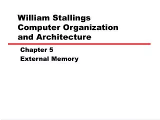
William Stallings Computer Organization and Architecture. Chapter 4 Internal Memory. The four-level memory hierarchy. ♦ Computer memory is organized into a hierarchy.

E N D
William Stallings Computer Organization and Architecture Chapter 4 Internal Memory
The four-level memory hierarchy ♦Computer memory is organized into a hierarchy. ♦Decreasing cost/bit, increasing capacity, slower access time, and decreasing frequency of access of the memory by the processor ♦The cache automatically retains a copy of some of the recently used words from the DRAM.
Memory Hierarchy • Registers • In CPU • Internal or Main memory • May include one or more levels of cache • “RAM” • External memory • Backing store
4.1 COMPUTER MEMORY SYSTEM OVERVIEW Characteristics of Memory Systems • Location • Capacity • Unit of transfer • Access method • Performance • Physical type • Physical characteristics • Organisation
Location The term location refers to whether memory is internal or external to the computer. • CPU • The processor requires its own local memory , in the form of registers. • Internal • Main memory, cache • External • Peripheral storage devices, such as disk and tape
Capacity Internal memory capacity typically expressed in terms of bytes(1byte=8bits)or words. External memory capacity expressed in bytes. • Word • The natural unit of organisation • Word length usually 8, 16 and 32 bits • The size of the word is typically equal to the number of bits used to represent a number and to the instruction length. Unfortunately, there are many exceptions.
Unit of Transfer • Internal • Usually governed by data bus width • External • Usually a block which is much larger than a word • Addressable unit • Smallest location which can be uniquely addressed • At the word level or byte level • In any case, 2A=N, A is the length in bits of an address N is the number of addressable units
Access Methods (1) • Sequential access • Start at the beginning and read through in order • Access time depends on location of data and previous location • variable • e.g. tape • Direct access • Individual blocks have unique address • Access is by jumping to vicinity plus sequential search • Access time depends on location and previous location • variable • e.g. disk
Access Methods (2) • Random • Individual addresses identify locations exactly • Access time is independent of location or previous access and is constant • e.g. RAM • Associative • Data is located by a comparison with contents of a portion of the store • Access time is independent of location or previous access and is constant • e.g. cache
Performance Parameters • Access time • For random-access memory • the time it takes to perform a read or write operation. • Time between presenting the address to the memory and getting the valid data • For non-random-access memory • The time it takes to position the read-write mechanism at the desired location. • Memory Cycle time • Cycle time is access time plusadditional time • Time may be required for the memory to “recover” before next access • Transfer Rate • Rate at which data can be moved
Physical Types • Semiconductor • RAM • Magnetic • Disk & Tape • Optical • CD (Compact Disk) & DVD (Digital Video Disk) • Others • Bubble • Hologram
Physical Characteristics • Decay • Volatility • In a volatile memory, information decays naturally or is lost when electrical power is switched off. • In a nonvolatile memory, no electrical power is needed to retain information, e.g. magnetic-surface memory. • Erasable • Power consumption
Organisation • Organisation means physical arrangement of bits into words • Obvious arrangementnot always used
Memory Hierarchy • Registers • In CPU • Internal or Main memory • May include one or more levels of cache • “RAM” • External memory • Backing store
The Bottom Line The design constraints on a computer’s memory: • How much? • Capacity • How fast? • Time is money • How expensive? A trade-ff among the three key characteristics of memory: cost, capacity, and access time.
Hierarchy List • Registers • L1 Cache • L2 Cache • Main memory • Disk cache • Disk • Optical • Tape
Hierarchy List Across this spectrum of technologies: • Faster access time, greater cost per bit • Greater capacity, smaller cost per bit • Greater capacity, slower access time From top to down: • Decreasing cost per bit • Increasing capacity • Increasing access time • Decreasing frequency of access of the memory by the processor
So you want fast? • It is possible to build a computer which uses only static RAM (see later) • This would be very fast • This would need no cache • How can you cache cache? • This would cost a very large amount
Locality of Reference • During the course of the execution of a program, memory references tend to cluster • e.g. loops and subroutines • Main memory is usually extended with a higher-speed, smaller cache. It is a device for staging the movement of data between main memory and processor registers to improve performance. • External memory, called Secondary or auxiliary memory are used to store program and data files and visible to the programmer only in terms of files and records.
4.2 Semiconductor Main Memory Table 4.2 Semiconductor Memory Types
Types of Random-Access Semiconductor Memory • RAM • Misnamed as all semiconductor memory is random access, because all of the types listed in the table are random access. • Read/Write • Volatile • A RAM must be provided with a constant power supply. • Temporary storage • Static or dynamic
Dynamic RAM (DRAM) • Bits stored as charge in capacitors • Charges leak • Need refreshing even when powered • Simpler construction • Smaller per bit • Less expensive • Need refresh circuits • Slower • Main memory
Static RAM (SRAM) • Bits stored as on/off switches • No charges to leak • No refreshing needed when powered • More complex construction • Larger per bit • More expensive • Does not need refresh circuits • Faster • Cache
Read Only Memory (ROM) • Permanent storage • Applications • Microprogramming (see later) • Library subroutines • Systems programs (BIOS) • Function tables
Types of ROM • Written during manufacture • Very expensive for small runs • Programmable (once) • PROM • Needs special equipment to program • Read “mostly” • Erasable Programmable (EPROM) • Erased by UV • Electrically Erasable (EEPROM) • Takes much longer to write than read • Flash memory • It is intermediate between EPROM and EEPROM in both cost and functionality. • Erase whole memory electrically or erase blocks of memory
Organisation in detail • Memory cell • The basic element of a semiconductor memory • Two stable states • being written into to set the state, or being read to sense the state Chip Logic • One extreme organization : the physical arrangement of cells in the array is the same as the logical arrangement. The array is organized into W words of B bits each. • e.g. A 16Mbit chip can be organised as 1M 16-bit words • One-bit-per-chip in which data is read/written one bit at a time • A bit per chip system has 16 lots of 1Mbit chip with bit 1 of each word in chip 1 and so on
Chip Logic • Typical organization of a 16-Mbit DRAM • A 16Mbit chip can be organised as a 2048 x 2048 x 4bit array • Reduces number of address pins • Multiplex row address and column address • 11 pins to address (211=2048) • An additional 11 address lines select one of 2048 columns of 4bits per column. Four data lines are for the input and output of 4 bits to and from a data buffer. On write, the bit driver of each bit line is activated for a 1 or 0 according to the value of the corresponding data line. On read, the value of each bit line selects which row of cells is used for reading or writing. • Adding one more pin devoted to addressing doubles the number of rows and columns, and so the size of the chip memory grows by a factor 4.
Refreshing • Refresh circuit included on chip • Disable chip • Count through rows • Read & Write back • Takes time • Slows down apparent performance
Chip Packaging EPROM package , which is a one-word-per-chip, 8-Mbit chip organized as 1M×8 •The address of the word being accessed . For 1M words, a total of 20 pins (220=1M) are needed. •D0~D7 •The power supply to the chip (VCC) •A ground pin (Vss) •A chip enable (CE) pin: the CE pin is used to indicate whether or not the address is valid for this chip. •A program voltage (Vpp)
DRAM package, 16-Mbit chip organized as 4M×4 RAM chip can be updated, the data pins are input/output different from ROM chip •Write Enable pin (WE) •Output Enable pin (OE) •Row Address Select (RAS) •Column Address Select (CAS)
Module Organisation ·If a RAM chip contain only 1bit per word, clearly a number of chips equal to the number of bits per words are needed. e.g. How a memory module consisting of 256K 8-bit words could be organized? 256K=218, an 18-bit address needed; The address is presented to 8 256K×1-bit chips, each of which provides the input/output of 1 bit. Figure 4.6 256kbyte memory Organization
Module Organisation (2) Figure 4.7 1-Mbyte Memory Organization
(1M×8bit/256K×8bit)=4=22 As show in figure 4.7, 1M word by 8bits per word is organized as four columns of chips, each column containing 256K words arranged as in Figure 4.6. • 1M=220 For 1M word, 20 address lines are needed. The 18 least significant bits are routed to all 32 modules. The high-order 2 bits are input to a group select logic module that sends a chip enable signal to one of the four columns of modules.
Error Correction • Hard Failure • Permanent defect • Soft Error • Random, non-destructive • No permanent damage to memory • Detected using Hamming error correcting code
Error Correcting Code Function •A function f, is performed on the data to produce a code. •When the previously stored word is read out, the code is used to detect and possible correct errors. •A new set of K code bits is generated from the M data bits and compared with the fetched code bits.
Even Parity bits Figure 4.9 Hamming Error-Correcting Code Figure 4.9 uses Venn diagrams to illustrate the use of Hamming code on 4-bit words (M=4). With three intersection circles, there are seven compartments. We assign the 4 data bits to the inner compartments. The remaining compartments are filled with parity bits. Each parity bit is chosen so that the total number of 1s in its circle is even.
Figure 4.8 Error-Correcting Code • The comparison logic receives as input two k-bit values. A bit-by-bit comparison is done by taking the exclusive-or of the two inputs. The results is called the syndrome word. • The syndrome word is therefore K bits wide and has a range between 0 and 2K-1. The value 0 indicates that no error was detected. Leaving 2K-1 values to indicate, if there is an error, which bit was in error (the numerical value of the syndrome indicates the position of the data bit in error). • An error could occur on any of the M data bits or K check bits so, 2K-1≥M+K (This equation gives the number of bits needed to correct a single bit error in a word containing M data bits.)
Those bit positions whose position number are powers of 2 are designated as check bits. Each check bit operates on every data bit position whose position number contains a 1 in the corresponding column position. Bit position n is checked by those bits Ci such that ∑i=n. C8 C4 C2 C1 Figure 4.10 Layout of Data bits and Check bits
The check bits are calculated as follows, where the symbol designates the exclusive-or operation: Assume that the 8-bit input words is 00111001, with data bit M1 in the right-most position. The calculations are as follows: Suppose the data bit 3 sustains an error and is changed from 0 to 1.
When the new check bits are compared with the old check bits, the syndrome word is formed: The result is 0110, indicating that bit position 6, which contains data bit 3, in error.
Figure 4.11 Check Bit Degeneration a single-error-correction (SEC) code
More commonly, semiconductor memory is equipped with a single-error-correcting double-error-detecting (SEC-DED) code. An error-correction code enhances the reliability of the memory at the cost of added complexity. Table 4.3 Increase in Word Length with Error Correction
1 1 Figure 4.12 Hamming SEC-DEC Code The sequence show that if two errors occur (Figure 4.12 c), the checking procedure goes astray (d) and worsens the problem by creating a third error (e). To overcome the problem, an eighth bit is added that is set so that the total number of 1s in the diagram is even.
4.3 CASHE MEMORY • Small amount of fast memory • Sits between normal main memory and CPU • May be located on CPU chip or module
Cache operation - overview Figure 4.14 Cache/Main-Memory Structure (P118) • Cache includes tags to identify which block of main memory is in each cache slot. The tag is usually a portion of the main memory address. Line Number Block Tag 0 1 2 C-1 Block length (k words) (a) Cache
Memory address 0 1 2 3 2n-1 Block (K words) Block Word Length (b) Main Memory
Figure 4.15 Cache Read Operation (P119) • CPU requests contents of memory location • Check cache for this data • If present, get from cache (fast) • If not present, read required block from main memory to cache • Then deliver from cache to CPU
Typical Cache Organization •In this organization, the cache connects to the processor via data, control, and address lines. •The data and address lines attach to data and address buffers, which attach to a system bus from which main memory is reached. •When a cache hit occurs, the data and address buffers are disabled and communication is only between processor and cache, with no system bus traffic •When a cache miss occurs, the desired address is loaded onto the system bus and the data are returned through a data buffer to both the cache and main memory. Figure 4.16 Typical Cache Organization
Elements of Cache Design • Size • Mapping Function • Direct • Associative • Set Associative • Replacement Algorithm • Least recently used (LRU) • First in first out (FIFO) • Least frequently used (LFU) • Random • Write Policy • Write through • Write back • Write once • Block Size • Number of Caches • Single or two level • Unified or split