Download
1 / 26
260 likes | 398 Vues
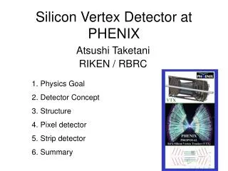
PHENIX Silicon Pixel Detector Construction, Operation, and the first Results. Atsushi Taketani RIKEN Nishina center RIKEN Brookhaven Research Center. Outline Detector Hardware Installation and Peripheral Operation and Physics result Issue and repair work Summary. History

E N D
PHENIX Silicon Pixel Detector Construction, Operation, and the first Results Atsushi Taketani RIKENNishina center RIKEN Brookhaven Research Center Outline Detector Hardware Installation and Peripheral Operation and Physics result Issue and repair work Summary History 2004.8 First proposal 2007.6 Start Construction 2008.8 Beam test at FERMILAB 2010.10 Barrel assembly start 2010.12 Installed and operation start
Requirements for Vertex Tracker Heavy Ion collision and polarized proton-proton up to CMS 200 / 500GeV Physics side • High precision tracking for displaced vertex measurement. • ct~ 100mm(D), ~400mm(B) • Large coverage tracking capability with momentum resolution (|h|<1.2 , and full azimuthally with s/P ~ 5%P) • High charged particle density ‘dN/dh’ ~ 700 @h=0 ~ 2000 Tracks • High Radiation Dose ~100KRad@10Years • High Luminosity 2*1032 cm-2 s-1@PP -> High rate readout • Low Material Budget <- avoid multiple scattering and photon conversion for electron measurement by outer detectors. Environment side
Silicon Vertex Tracker e Life time (ct) D0 : 123 mm B0 : 464 mm Layer 3 e+ DCA e- Layer 2 D Beryliumbeampipe p p Layer 1 B Layer 0 e Strip 3 Strip2 pixel1 pixel0 VTX: Silicon Barrels ~ 2p Pixel : inner 2 layers and Stripixel: outer 2 layers
Pixel Detector 57mm (32 x 4 pixel) 13mm 256 pixel 50mm x 425mm Sensor module Pixel bus SPRIO Pixel sensor modules Pixel stave (with cooling) Full ladder Pixel detector = inner 2 layers of VTX 1st layer: 10 full pixel ladders = 20 half ladders = 40 sensor modules 2nd layer: 20 full pixel ladders = 40 half ladders = 80 sensor modules ~4mm 5
PIXEL (Sensor and Readout, bump bonded) • Readout by ALICE_LHCB1 chip • Amp + Discriminator / channel • Bump bonded to each pixel • Running 10MHz clock ( RHIC 106nsec ) • Digital buffer for each channel > 4msec depth • Trigger capability > FAST OR logic for each crossing • 4 event buffer after L1 trigger Pixel size( x z)50 µm x 425 µm Sensor Thickness 200mm r = 1.28cm, z = 1.36 cm (Active area) 256 x 32 = 8192 channel / sensor 4 chip / sensor 4 sensor / stave Total 4M Pixel
Reaout overview Analog Pilot ASIC OE / EO F P G A DATA Analog Pilot Digital Pilot GOL Digital Pilot ASIC CTRL CTRL Digital Pilot ASIC OE / EO GOL CTRL GOL Analog Pilot ASIC FPGA CTRL CLK GOL Digital Pilot Analog Pilot 32 bit 32 bit 2 2 2 2 1 1 1 1 32 bit 32 bit Readout scheme In order to meet the PHENIX readout speed requirement, parallel readout (4 x 32 bit) was made. parallel 4 x 32 bit at 10 MHz SPIRO Module • Digital Pilot Chip • Receiving 4 x 32 bit data from R/O chips • Sending data to FPGA • Controlling R/O chips • Analog Pilot Chip • Supplying reference voltage for R/O chips. • Monitoring supply, bias voltage and temperature on the detector. • GOL : Transmit data with 1.6 Gbps • Number of data lines is 128 ( 4 x 32 bit) • Readout time is 256 (f) x 2 chips x 10 MHz = 51.2 ms 7
Through hole Wire bonding Signal layer Al Power Al GND Sensor module Thermo-plate Signal 1;(for Surface Mount Device) Signal-1 to Signal-4are connected with through hole Bus structure • 6 layers structure • GND, Power and 4 signal lines Total 188 lines 25cm long 1.4cm wide Final configuration Signal-1 3 mm Cu Signal-2 3 mm Cu Signal-3 3 mm Cu Signal-4 3 mm Cu Signal 2;(Vertical line)line connected withpixel chip with wire bonding Power 50 mm Al Signal 3;(Horizontal line)send signal to Pilot Module connected with vertical line with through hole Signal 4;(for manufacture reason) GND 50 mm Al Signal lines; 60 mm pitch Material Budget; Total ~ 0.26 % 8
Procedure 3 3. Align each sensor module 5μm
Encapsulation of wire barrier Potting glue 1mm Bonding wire sensor stave Cross section Resonance No encap ~5.9KHz Side view of bonding wire • Wire has intermittent current due to readout synchronized the level 1 trigger. • Wire vibrates in magnetic field and may break
Beryliumbeampipe Layer 0 (PIXEL) 5 ladders Layer 1 (PIXEL) 10 ladders Completed and installed on 2011.12
VTX System Cooling tube FEM Optical cable Flow Sensor Pixel/Strip Detectors Thermo- sensor Sensor cable Power cable Interlock System Chiller Power Supply • To remove power dissipation 1560W/VTX, need to cool down pixel/strip detectors. • To avoid detector destruction by heating, need safety interlock system • Interlock trips off power supply by temperature and flow of coolant. 13
Pixel ladder as of 2011 January 15 Q/A test by Asano and Akimoto West bottom West L0 Central Arm West top West bottom West L1 West top East top East L0 Central Arm East bottom East top Central Arm Acceptance Central Arm Acceptance East L1 East bottom Compiled by H. Asano
PHENIX-VTX in Action at RHIC VTX in Run 2012:p+pat 200 GeV VTX in Run 2011:Au+Auat 200 GeV Primary Vertex: BBC vs VTX Data: AuAu at 200 GeV y (cm) Beam size s (beam) ~ 90 um x (cm)
Pixel at PHENIX VTX completed • Since 2011.12, Operation started. • We archived • Large acceptance |h| < 1.2, Df~2p • Primary vertex resolution(DCA) s ~ 77mm • b->e and c->e separation • Issues: Damage to wires of pixel detectors during 1st run
Bus side 5mm long Chip side • Large temperature excursion due to the cooling interlock broke wires. • Wire breaks at neck. -> not problem on wire bonding, problems on extra tensions • 5-10deg -> -5deg for a few minibus, by turning off power ~ 1W/cm2, but running cooling system • Expansion coefficient Encapusulant ~ 300ppm/deg(Sylgard184 and 186) • Other material ( Myler, Si, Al, Cu Carbon ) 20~30ppm/deg
Reapir • Removing encapulant • Clean up pad • But fear to damage pad • Decide wire on bond mark. • After re-wire bonding, pull tests were performed. • Always neck breaks with 6-8g tension.
Actions and Repairing work • Fix interlock system, minimize unnecessary LV off. • Operate 15-20deg, to decrease thermal shock. • No additional broken wire. • Repair work • Remove encapsulant • Clean up bonding pad • Re-wire bonding • encapsulation • Encapsulant • Available encapsulation material 300ppm/deg • Use soft material to minimize extra tension. • Penetration 65 (JIS K2207) • Survive Heat shock test ( 0<->40deg 1min 50 times)
Summary • We constructed Si Pixel detector for heavy ion collision experiments. • It works and performs well for physics • Vertex resolution 77mm. • Some of pixel ladders were damaged in the first run. Repair work is underway
VTX parameters (in proposal) Pixel detector Strip detector BEAM Pixel Strip