Verification of the Cell Broadband Engine™ Processor
60 likes | 65 Vues
Verification of the Cell Broadband Engineu2122 Processor

Verification of the Cell Broadband Engine™ Processor
E N D
Presentation Transcript
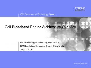
20.2 Verification of the Cell Broadband Engine™ Processor Kanna Shimizu1, Sanjay Gupta1, Tatsuya Koyama2, Takashi Omizo3, Jamee Abdulhafiz1, Larry McConville1, Todd Swanson1 1 IBM Corporation, Austin, Texas, 2 Sony Computer Entertainment Inc., Tokyo, Japan, 3 Toshiba Corporation, Ohme, Japan ABSTRACT Successfully developing an implementation of entirely new chip architecture such as the Cell Broadband Engine™ (Cell BE) processor from scratch is a notable achievement. Consider further the design complexity (234 million transistors) and the project management complexity (5 participating companies, work in 5 different time zones), and the task seems quite challenging. This paper describes how the central verification team staffed by Sony Computer Entertainment Inc. (SCEI), Toshiba Corporation, and IBM, produced on first silicon a Cell BE microprocessor functional enough to boot an operating system and run applications. For example, the heterogeneous multi- processor architecture required new multi-processor verification strategy and tools. The Cell verification activity was indeed built from the ground-up. However, on a positive note, this afforded us an opportunity to rethink our verification strategy without being hampered by legacy code. Starting with a somewhat clean slate, we developed new methodologies and approaches such that, just like the Cell architecture, there are many “firsts” in verification. For example, it is the very first time IBM has used an outside vendor tool as its central verification tool for a large design project. Conversely, the vendor had never had their tool used on such a large chip as Cell, and consequently, the Cell verification team collaborated with the vendor on many tool technology advances, including performance and SoC verification methodology and feature definitions. Categories and Subject Descriptors B.5.2 [RTL Implementation]: Design Aids In addition, the fact that the Cell design center is staffed from three companies, SCEI, Toshiba, and IBM (hence the name STI Design Center), created an opportunity for a mixing of verification methodology DNA. Needless to say, the three companies came in with varied verification methodology experiences and philosophies. General Terms: Management, Verification. Keywords: Processor reference model, Directed random verification, Hierarchical verification, Trace-based verification 1.INTRODUCTION The Cell BE [PAB05], a supercomputer/system-on-a chip, is one of industry’s most advanced design with a host of features, many of which are “first-time” features: a heterogeneous multi- processor architecture, a new processor named the Synergistic Processing Element (SPE) [FAD05], a custom high-speed chip interface designed specifically for this architecture, and a security architecture , to name a few. Summary: This paper is a study of the techniques that were especially effective or even critical for the success of the first Cell BE chip tapeout. It is not intended to be a thorough overview of our verification methodology or our verification design flow. In fact, it can be safely assumed that if a particular technique is not covered in this paper, that it only had limited impact. In particular, simulation-based techniques were far more effective than formal-based techniques (formal techniques found only 0.2% of the bugs). The paper will focus on specific techniques and topics that had an impact such as hierarchical verification, random verification, and trace-based architectural verification. Since the architecture is so new, the team could not rely on reusing or extending an existing verification code base of tests and checkers. Instead vast amounts of new verification code needed to be created from scratch. This not only applies to the requisite tests, checkers, and coverage code, but also to something as fundamental as a reference model for the SPE Instruction Set Architecture (ISA) for example. The reference model, which is critical as a backend for test generators and checkers, did not exist at the beginning of the project and needed to be developed in parallel with the ISA development. Additionally, the team could not rely on pre-existing methodologies straight out of the can. 2.BACKGROUND Cell BE Architecture The Cell BE is a multi-core architecture with the following primary components: the PowerPC Processor Element (PPE), eight SPEs, the Element Interconnect Bus (EIB), the Memory Interface Controller (MIC), and the Bus Interface Controller (BIC). The primary function of the PPE is the management and allocation of tasks for the SPEs. The SPEs are targeted for tasks that require high computational unit density and are intended to fill the void between general-purpose processors and special-purpose hardware. The EIB is a memory coherent bus connecting the processor cores to each other and with the interface controllers for the off-chip main memory and the I/O Southbridge. Permission to make digital or hard copies of all or part of this work for personal or classroom use is granted without fee provided that copies are not made or distributed for profit or commercial advantage and that copies bear this notice and the full citation on the first page. To copy otherwise, or republish, to post on servers or to redistribute to lists, requires prior specific permission and/or a fee. DAC 2006, July 24-28, 2006, San Francisco, California, USA. Copyright 2006 ACM 1-59593-381-6/06/0007…$5.00. 338
the software simulator that software developers use to develop code for a Cell BE based platform [SDK05]; for SPU logic verification, it is used in the directed random processor instruction generator for test case creation, and it is also embedded in the SPU behavioral checker. As described in [WAT06], the code reuse not only expedited the verification at many different levels, but also, because there was one central model, frequent changes to the ISA were well-absorbed by the various teams. The SPU reference model was one critical key to the success of the new processor architecture. SPU SPU SPU SPU … … LS MFC LS MFC LS MFC LS MFC PPE PPE SPE0 SPE0 SPE7 SPE7 Bus (EIB) Bus (EIB) Bus Interface Controller Bus Interface Controller (BIC) (BIC) Memory Interface Memory Interface Controller (MIC) Controller (MIC) Also, [JAC05] describes the formal verification work on the SPU floating point unit. The floating point datapath was proven equivalent to a high-level reference model, giving confidence that the design was clean. To Southbridge Chip or to another Cell Chip to another Cell Chip To Southbridge Chip or To Main Memory To Main Memory 3.HIERARCHICAL VERIFICATION One of the key reasons for the team’s success can be attributed to the astute use of hierarchical verification. Throughout the project, verification work was happening in parallel on various design targets ranging from a single block (designed by a single designer) to the full Cell chip. In fact, there were in total 30 environments (defined by the “design under verification” and the accompanying verification code): the full chip, 2 Cell chips, the PPE, the SPE, the SPU, the MFC, the MIC, and the BIC to name a few. Figure 1 Cell BE Architecture Each SPE includes the Synergistic Processor Unit (SPU), the Memory Flow Controller (MFC) which is a data transfer engine, and the Local Storage (LS) which is 256K of on-chip memory. The SPU fetches instructions from the LS and load/stores data to and from the LS. However, LS is not a hardware-managed cache but rather a memory region mapped in the system memory address map and managed explicitly by software. The MFC provides the primary method for data transfer, protection, and synchronization between LS and main storage. The MFC presents two types of interfaces: one to the SPU (for processing the SPU’s data transfer commands) and another to all other processors and devices (via the bus). It can support multiple memory accesses in flight and data transfers initiated by both the SPU and the PPE. ?Multi-processor correctness correctness ?Multi-processor Cell, 4 SPE Cell Cell, 4 SPE Cell SPE, PPE SPE, PPE ?Connectedness ?Connectedness ?Interface assumption ?Interface assumption validation validation SPU SPU BIC BIC MFC MFC With previous and most other multi-core chip architectures, the processors are symmetric and memory accesses are simply between each processor and main storage(s). These memory accesses can be thought of as parallel “pipes”. In contrast, the processors in the Cell BE are asymmetric and have a master-slave relationship; memory accesses happen not only between each processor and main storage, but also from the PPE to SPE and from one SPE to another SPE. Thus, instead of parallel pipes, the formation is closer to an intersecting web of pipes. From the MFC perspective, there are LS accesses that were initiated from its own SPU, but also simultaneously it must be able to manage LS accesses from the other cores on the chip. This feature alone should make it clear how verification innovation was necessary to thoroughly verify this new architecture. PU PU MIC MIC ?Processor element functionality validation functionality validation ?Processor element EIB EIB Unit/Island Environments Unit/Island Environments Found 95% of Bugs Found 95% of Bugs ?Thorough coverage ?Thorough coverage ?Functionality testing ?Functionality testing Partitions: 0.2% of Bugs Partitions: 0.2% of Bugs 30 Simulation Environments Environments 30 Simulation Full Chip: 3.5% of Bugs Full Chip: 3.5% of Bugs Verification Environment Hierarchies Verification Environment Hierarchies Figure 2 Hierarchical Approach As it is clear from the architecture overview, many new aspects of the chip are focused on the SPE and the interactions of the rest of the chip with the SPE. Consequently, many of the new verification challenges that were faced center on the SPE, and our strategies for addressing these challenges are a focus of this paper. A parallel approach is taken because each verification environment is well-suited to find a particular class of bugs, and no single environment is capable of catching all types of bugs. Accordingly, the verification objectives, scope, and techniques differ for each hierarchy of environment. The full chip environment for example, focuses on finding multi-processor and memory coherency bugs while a smaller design block’s environment will focus on functionality, coverage, and thorough exercising of the logic. In fact, although management tends to rely on the status of full chip testing to gain reassurance that the chip Other Cell BE Verification Publications As noted in the Introduction, an executable SPU reference model was coded from scratch in order to develop the SPU ISA (in contrast to the PPE core which had a PowerPC reference model from previous projects). This SPU reference model [WAT06] was so well- designed that it was re-used for a multitude of tasks; it is used in 339
bugs as possible. The full chip (or any larger) environment should be used only to find one, interaction bugs that appear when two units are put together, and two, bugs that are due to incorrect unit interface assumptions. is functional, there are many bugs that can only be found in the smaller environments. And there are many tests, especially those which target specific functionality, that can only be run in the smaller environments because a larger environment’s simulation efficiency would make it impractical. Therefore, completion of full chip testing did not indicate the end of Cell verification work because testing in many other environments are orthogonal to and of equal importance as the full chip testing. The Cell verification team was able to realize this strategy; roughly, 95% of the bugs were found in the smaller “Island” or “Unit” environments (this includes environments of the sizes of MFC-only or SPU-only and also smaller logic units that constitute the SPU for example), 0.2% of the bugs were found in the “Partition” environments (environments of the scope of the SPE and the PPE), and finally, 3.5% of the bugs were found in the full chip environment. And, many of the bugs found in the full chip environment could only have been found with the entire chip logic. Phase1 CHIP PH2 PH3 PH4 PH5 PH1 Phase3 Phase4 Phase5 PH4 PARTITION PH2 PH3 PH5 PH1 Another important aspect of hierarchical verification is that smaller environments can typically run longer test cases; for example, MFC test cases can comfortably run an order of magnitude longer (i.e. more design clock cycles for a single, continuous test case) than a full chip test case. This is critical because some bugs require such a long event sequence in order to manifest itself, that only the smaller environment with its long running test case can reach that scenario. The verification team found many bugs in the smaller environments that could not have been found in the chip environment for this reason. Thus, it was critically important that the smaller environment verification continues even after the full chip environment was up and running so that the long random test cases can find more bugs. In fact, although the limitation on the running time of the full chip random test cases was a concern, no bugs have been found post- silicon that could have been found with a longer chip test case. This can be attributed to the long, small environment test cases successfully finding many of the bugs pre-silicon. Phase2 PH2 Phase3 PH3 Phase4 PH4 Phase1 PH1 ISLAND PH5 UNIT PH3 PH4 PH5 PH1 PH2 Time Figure 3 Parallel Strategy on All Hierarchies Compared to previous IBM projects, the Cell verification team made a heavier use of this parallel strategy. Figure 3 displays how the various hierarchies overlapped in their verification efforts (the different phases are scaled in the diagram to indicate the actual time spent to achieve criteria milestones.) In previous projects, the hierarchy approach was more sequential; as verification work on the smaller blocks neared completion, only then did testing begin on larger parts of the chip. However, with the vast amount of verification work needed for a brand new architecture and design, the Cell team needed to compress the effort into a limited schedule and thus, they found the parallel strategy very effective; the different sized environments were all productive for finding bugs right up to tapeout. In fact, out of the bugs found during the 1 month before tapeout, 6 out of 7 were found in the smaller environments, and only 1 was found by the chip environment. Summary One key reason for the team’s success can be attributed to its excellent usage of hierarchical verification. First, the team accomplished the goal of finding the majority of the bugs with the smaller, faster environments. This leads to a high rate of bugs found per unit engineer’s time, per unit simulation time, and frees the larger environment tests to accomplish their true mission. This efficiency metric is especially critical for a large chips with multiple cores such as the Cell BE, and in general, as designs become larger and multi-core becomes more of a prevalent architecture, this should become a key point industry-wide. Second, because smaller environment simulation continued in parallel with the larger environment simulation, the design was more thoroughly simulated and more corner case scenarios were hit than with a sequential approach where small environment testing tapers off. It is critical to understand that different-sized verification environments each find a mutually exclusive class of bugs. As schedules become more compressed while chip complexity grows, this parallel hierarchical approach should become more and more of a necessity. Another key difference with previous projects is the number of hierarchies. There were more intermediate level environments than with past approaches. These are the hierarchies that we have: unit, island, partition, chip, system. This strategy is similar to how in processor architectures, pipeline stages are added to increase parallel processing. With more levels of environments, the Cell verification team was able to concurrently verify a wider range of simulation scope. The value of the parallel approach can be appreciated by understanding the simulation efficiency differences among the environments. Because of its sheer size, full-chip simulation takes much longer than simulating a single block. For example, the SPU-only logic can simulate roughly 12 times faster than the full chip logic for the same number of design clock cycles. This difference is significant because typically test cases are rerun several times to debug and isolate the problem and to verify the fix. Thus, one can conclude that simulation cycles should be spent on the more efficient SPU environment to root out as many 4.RANDOM VERIFICATION Another characteristic of the Cell team’s approach is its heavy emphasis on random-based stimulus generation. A typical Cell verification environment includes a random-based stimulus on the input side and a checker that observes and verifies the actions continuously on the output side. This is in contrast to a typical self-checking testcase where the stimulus is static and the 340
random stimulus and scenario generation on many different levels was a key factor in producing clean logic from ground zero. In particular, random verification at the chip level is discussed here in detail. checking is done by the testcase on just the end result. Note that although the random simulation requires investment in developing a sophisticated checker which can discern incorrect behavior in a variety of scenarios, there are many benefits. Once the stimulus generator and the checker are implemented, it can be run repeatedly with different initial values for the random generator and with different weighting of constraints. Thus, many scenarios can be explored with very little manual intervention. Furthermore, a checker that continuously checks the design’s actions greatly cuts down on debug time compared to an end-of- test check because the checker will flag an error as soon as it happens. 4.1Chip-Level Random Verification X-Gen The test cases for chip-level verification are generated using IBM’s X-Gen test generator [EME02]. X-Gen is a directed random test generator for system-level transactions. It pre- generates sequences of processor instructions based on user specified constraints. For the Cell processor, X-Gen was extended for the SPE processor architecture and its interaction with the PowerPC based PPE. Since the Cell BE is a multi-core design, chip level verification is effectively multiprocessor verification, and X-Gen effectively handles this challenge. The tool outputs instruction sequences for the processor cores, the PPE and one or more of the SPEs, to execute concurrently so that interesting collisions occur. X-Gen also creates event sequences for the I/O connection port (used to connect to the Southbridge or a second Cell chip) to emulate incoming traffic from off-chip. For random verification, coverage tracking is critical from a project management perspective. The Cell team was able to effectively use coverage information to see saturation of the random testcases. Figure 4 indicates coverage convergence of various units, the chip environment, and the system environment. Coverage 120 % C o v e ra g e 100 80 60 40 20 0 … … Time 1 Time 3 Time 5 Time 7 Time 9 Time 11 Time 13 Time 15 Time 17 Time 19 Time 21 Time 23 Time 25 Time 27 Time 29 PPE PPE SPE0 SPE0 SPE7 SPE7 EIB EIB Time Bus Interface Controller Bus Interface Controller (BIC) (BIC) Memory Interface Controller (MIC) Controller (MIC) Memory Interface Unit 1 Unit 2 Unit 3 Chip System Cell Cell Figure 4 Coverage Convergence for Environments X-Gen generated X-Gen generated instruction stream instruction stream Possible Transactions Transactions Possible Granularity of input randomization Granularity of input randomization Tools Tools Figure 6 X-Gen and Stimulus Generation ?IBM RuleBase ?IBM RuleBase [RB97] [RB97] Signal level Signal level Individual signals are toggled in a constrained (following protocol) Individual signals are toggled in a constrained (following protocol) random fashion. random fashion. X-Gen primarily focuses on DMA (Direct Memory Access) transactions. Although, the PowerPC architecture has 600+ instructions, X-Gen supports about a third of those; for example, arithmetic and logical instructions are not supported. Users can specify any of the supported instructions as well as interactions which are abstract levels of transactions. An example of an interaction is a SPE generated DMA to main system memory, where the “interaction” is between the initiating SPU and the target memory. ?IBM SixthSense [SS05] [SS05] ?IBM SixthSense ?External ?External vendor tool vendor tool Transaction level Transaction level Bus transactions are randomized on command, address, and data, to Bus transactions are randomized on command, address, and data, to exercise the MFC. exercise the MFC. ?Internal C++ ?Internal C++ based tool based tool ?GPRO ?GPRO [GPRO95] [GPRO95] Instruction level Instruction level Instruction sequences for the PowerPC PPE and the new SPE are generated in a directed random manner to hit corner cases. manner to hit corner cases. Instruction sequences for the PowerPC PPE and the new SPE are generated in a directed random There are numerous fields within the DMA interaction which the user can define to direct the test, including which of the eight SPE is the initiator, the source SPE Local Store address, the target memory address, the DMA transfer size, and the DMA command type. Any interaction field that is not specified will be randomly set by X-Gen based upon empirical testing knowledge. For example, if the address is left blank, X-Gen will try to pick an address that will cause interesting scenarios, such as an address at the end of a cache line or an address that had been previously requested so that there is access contention. In other words, X- ?XGEN ?XGEN [EME02] [EME02] Figure 5 Random Verification of Various Types The Cell team’s usage of random verification was not only pervasive but also existed at many different levels of granularity. Randomness is used at the signal level; it is used at the transaction level; it is also used at the instruction level. This pervasive use of 341
SPE Local Store location from the PPE and other SPEs, do indeed work correctly. Gen is capable of directing the test on its own instead of simply randomizing unspecified fields. This allows for a high degree of automation and user productivity. Furthermore, it is instrumental in generating meaningful tests that hit corner cases instead of wasting precious simulation cycles on repetitive ineffective testing. Thus, X-Gen was a key factor in verifying the innovative PPE/SPE multi-processor architecture within the scheduled time. SPU SPU 1. DMA Command Command 1. DMA Checking X-Gen does not have a Cell BE reference model, and so, it cannot predict the results of a test. Take a simple example of a test case where all the processors want to store to the same address in memory. The memory target will arbitrate to let one processor have access, and the remaining processors will have to wait for the first processor to complete. Without a reference model, it cannot be predicted which processor completes first and which processor completes last, and consequently, the final results in memory cannot be predicted. Therefore, instead, the chip level verification methodology relies on two checking methods, entirely decoupled from X-Gen, to check that the chip- level behavior is correct. One, unit-level, run-time checkers used in the smaller environments are inherited into the chip verification environment. Second, a trace-based checker that verifies architectural correctness is developed specifically for the chip environment; this verification technique will be described in more detail below. LS LS MFC MFC 3. Bus Command with Data with Data 3. Bus Command 2. LS Data Readout Readout 2. LS Data 4. To the MIC MIC 4. To the EIB EIB Figure 7 Event Sequence for a DMA transaction CML checks are executed at the end of simulation on the event traces that were generated during simulation. A trace tracks data flow from the source to destination passing through multiple units of the chip. As one example, here are some of the CML checkers that operate on a SPU generated DMA command which stores data to a cacheable memory location. First, there is a checker to match up a SPU processor instruction to a DMA command to the DMA controller, the MFC. Second, a check ensures that the parent DMA command has all of the correct corresponding decomposed commands. Then, the LS access for the data is checked. The LS which is multi- ported memory can receive read requests from multiple interfaces. An accountability check ensures all LS events are matched to one and only one of the possible read types. Next, the transaction is matched to the corresponding bus command on the EIB. At this point, the checker enforces ordering of the DMA command with respect to other DMA commands. As the bus command reaches the Memory Interface Controller (MIC), the EIB trace is matched to the MIC trace. Finally, in order to ensure the cache consistency of this cache line for subsequent transactions, a CML checker verifies that all caches have their copies of this address invalidated. X-Gen Results Several bugs, especially multi-processor memory coherency problems, were effectively exposed by X-Gen. Although LS is not a cache, each SPE does have a very small cache for atomic commands and translation fetches. Thus, the PPE and the SPEs act as an N-way system where they arbitrate on the EIB bus for shared addresses. One bug that caused the EIB to livelock was detected by the following X-Gen scenario. The PPE and SPE processors are competing for a single cache line in memory, with each processor trying to lock it by completing an atomic store to the cache line. After the line is locked by one processor, the other processors loop reading that cache line until the processor with the lock releases it by completing another store to this cache line. With this particular bug, under certain conditions, the store which would release the line was infinitely starved on the EIB because of the reads to the same cache line from the other looping processors. This bug, which was ultimately fixed by a design fix in the EIB, only manifested itself under a tight corner case scenario and was exposed after months of random simulation using the same X-Gen test case. This example exemplifies the importance and value of directed random stressing using X-Gen at the chip level. CML Results There are 40 new classes of checkers, in 25,000 lines of C++ code, written specifically for the Cell architecture. The CML checkers caught a total of seven bugs; all of these bugs are in the new areas of the architecture. The quality of these bugs are very high since they would have resulted in severe data integrity problems or ordering violations that would have prevented the realization of the customer specified programming platform. 5.TRACE-BASED VERIFICATION Although much bug-finding can be done with the intensive unit- level verification, at the end of the day, there must be end-to-end, chip-wide checking to ensure that the architect’s design intent for this brand new architecture is correctly implemented. Coherency Monitor Late (CML) [CML02] serves as this architectural enforcer, and it is the primary tool to verify that the designed chip complies with the Cell BE Architecture. One of these bugs is of special interest because it is an architecture bug that required changes in the architecture document. The bug was a discrepancy between Cell DMA architecture and PowerPC architecture. Although the Cell architecture is new, many aspects of it are modeled after the PowerPC architecture to inherit Multiprocessing (SMP) legacy, and thus, PowerPC ordering rules must be enforced. One particular PowerPC rule requires transfers to the same real address from the same thread to occur in order. In the case of SPE DMA list transfer, a DMA command is applied to a list of incrementing virtual addresses. Since multiple virtual addresses can be aliased to an identical real address, the list may contain multiple accesses to the same real address. However, the its rich Symmetric While unit verification focuses on unit attributes, CML focuses on global properties. In particular, CML checkers focus on data flow and ordering rules which are at the center of multi- processing correctness. CML checkers guarantee that innovative architectural features such as the capability to access an arbitrary 342
designed logic allowed the accesses in the list to be reshuffled and thereby not maintaining the PowerPC ordering rule. This bug was found by applying a pre-existing set of PowerPC CML checkers to the new architecture. 7.ACKNOWLEDGEMENTS The authors would like to thanks these people who gave it their all for this chip’s success: Salim Ahmed, Bill Tiernan, Gilles Gervais, Kenichi Takagi, Steve Roberts, Chris Spandikow, Hidenori Matsuzaki, Anush Rangarajan, Yukio Watanabe, Masaaki Nozaki, Jim Mikos, Hideyuki Saito, Lyle Grosbach, Richard Anderson, Andy Petruski, John Troppy, and many others. Because of its global nature, CML checkers are effective in finding bugs that are not caught by the unit checkers both in the unit environments and also in the chip environment. As an example, consider this bug that involved data flow through several units. For a particular type of DMA command, data is transferred from one unit to another and eventually to the LS. Although the full 128 byte full cache line is expected to be transferred to the LS, only 16 bytes was being transferred. The localized checks at the units and at the interfaces did not catch this bug. In contrast, a CML checker, which abstracts away details such as the multi-ported access to the LS memory to focus purely on the architecture, caught the incomplete transfer. To be precise, the bug was detected when a subsequent read result of the data at this address in simulation did not match the data in CML’s memory model of the LS. With its clean focus on global architecture, CML checkers are able to catch bugs that can be easily overlooked by localized and discrete unit checkers. CML was an indispensable tool in ensuring that the new Cell BE Architecture was indeed realized. 8.REFERENCES [PAB05] D. Pham et al. The Design and Implementation of a First-Generation CELL Processor. In IEEE International Solid- State Circuits Symposium, February 2005. [FAD05] B. Flachs et al. The Microarchitecture of the Streaming Processor for a CELL Processor. In IEEE International Solid- State Circuits Symposium, February 2005. [WAT06] Y. Watanabe et al. An SPU Reference Model for Simulation, Random Test Generation, and Verification. In IEEE Asia and South Pacific Design Automation Conference, January 2006. [SDK05] www-128.ibm.com/developerworks/power/cell/ [JAC05] C. Jacobi et al. Automatic Formal Verification of Fused- Multiply-Add FPUs. In IEEE Design Automation and Test in Europe Conference, March 2005. 6.CONCLUSION Overall Result The Cell design was simulated for over 2 trillion cycles before the chip was taped out for the first time. This sounds like a lot, but it translates to just 156 seconds of hardware operation time using the product clock frequency of 3.2 GHz. Therefore, it was especially critical to optimize the use of the simulation cycles to root out all the bugs including the corner case problems. After executing 780 million simulation tests, many of the bugs were detected. When the first Cell chip hardware came back, it immediately booted an operating system and ran applications. There were very few bugs that escaped verification into the first pass hardware. Analysis of these bug escapes showed that they required long and directed sequences of transactions with a very low probability of occurring in simulation; they are essentially bugs meant to be found in lab testing. One example is a data corruption error involving an abnormally long latency for the bus grant. In fact, even with lab testing, it was only exposed in a dual Cell system where latencies are longer. As this bug was not even seen in lab tests on a single Cell system, it is unlikely that it would have been found in any random simulation test no matter how long the simulation ran. [EME02] R. Emek et al. X-Gen: A Random Test-Case Generator for Systems and SoCs. In IEEE International High Level Design Validation and Test Workshop, 2002. [CML02] Ludden et al. Functional Verification of the POWER4 microprocessor and POWER4 multiprocessor system. In IBM Journal of Research and Development, Volume 46, Number 1, 2002. [SS05] Gott et al. Functional Formal Verification on designs of pSeries microprocessors and communication subsystems In IBM Jounal of Research and Development, Volume 49, Number 4,5, 2005. [RB05] RuleBase: Model Checking at IBM. In Computer Aided Verification (CAV), 1997. [GPRO95] Aharon et al. Test Program Generation for Functional Verification of PowerPC Processors in IBM. In Design Automation Conference (DAC), 1995. 343