
E 3
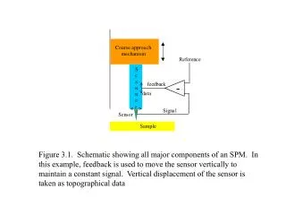
Figure 3.1. Schematic showing all major components of an SPM. In this example, feedback is used to move the sensor vertically to maintain a constant signal. Vertical displacement of the sensor is taken as topographical data. z. E 3. 3. 2. x. 1.

E 3
E N D
Presentation Transcript
Figure 3.1. Schematic showing all major components of an SPM. In this example, feedback is used to move the sensor vertically to maintain a constant signal. Vertical displacement of the sensor is taken as topographical data
z E3 3 2 x 1 Figure 3.2. Deformation of piezoelectric material in an electric field and the defining coefficients.
Z • Y • X Figure 3.3. Tripod design of SPM scanner with the sensor tip located at the bottom.
Figure 3.4. Tube scanner. (From Ref. 6 by permission of American Institute of Physics.)
Figure 3.5. An example of an inertia motor used for coarse approach in SPM.
Figure 3.6. One possible waveform for the inertia motor. The carrier is first pushed with a near constant speed and then the rail withdraws with great acceleration to cause slipping. The carrier will move in opposite direction by reversing the voltage polarity.
Figure 3.7. Left: Constant current mode, with feedback turned on to maintain a constant tunneling current. Right: Constant height mode, feedback is turned off. (From Ref. 8 by permission of American Institute of Physics.)
Figure 3.8. Schematic for the feedback loop used in constant current mode of STM.
Figure 3.9. Tunneling of a single electron through a potential barrier.
Figure 3.12. The density of states of superconducting Al. One of the first obtained by tunneling spectroscopy. The peak position roughly estimates . (From Ref. 9 by permission of American Physical Society.)
Figure 3.13. Formation of vortices in a superconductor. S region is still superconducting, but the area where the field penetrates (N) has now become normal (vortex core).
Figure 3.14 . STM vortex image of NbSe2 taken at 1.8K, with an external field of 1T. (From Ref. 11 by permission of American Physical Society.)
Figure 3.15. Co atoms on smooth Cu(111) surface. The Co atoms are moved to the desired pattern by carefully manipulating the position and voltage of the STM tip. Note how the electron waves in the background are being focused by the boundary. Lower pictures are dI/dV images of the top ones. (From Ref. 12 by permission of Macmillan MagazinesLtd.)
Figure 3.16. Potential energy between tip and sample as a function of the distance between them. The potential is attractive when they are far apart (non-contact), but it will become strongly repulsive when they are close together (contact).
Figure 3.17. A SiO2 AFM cantilever fabricated by photolithography. (From Ref. 13 by permission of American Institute of Physics.)
Figure 3.18. A laser optical system used to measure the deflection of the cantilever. This method is commonly used in many AFMs. (From Ref. 14 by permission of American Institute of Physics.)
Figure 3.19. Schematics for PSD. Arrows indicate displacement of the laser spot. (a) A simple PSD can only measure vertical displacement. (b) A quad-PSD can measure both vertical and lateral displacement.
Figure 3.20. A fiber optical tip used as a light source. The tip end is placed very close to the sample surface. (Reproduced with kind permission of L. Goldner and J. Hwang)


![[E;+] Example:S 3 ={e, 1 , 2 , 3 , 4 , 5 }](https://cdn2.slideserve.com/3765895/slide1-dt.jpg)