Download
1 / 8
80 likes | 192 Vues
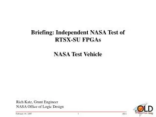
Briefing: Independent NASA Test of RTSX-SU FPGAs NASA Test Vehicle. Rich Katz, Grunt Engineer NASA Office of Logic Design. Top Level Block Diagram. 1,236 Stage Delay Line. 1,235 Inverter Chain Delay Line. Ripple Counter. For ATE Test.

E N D
Briefing: Independent NASA Test of RTSX-SU FPGAsNASA Test Vehicle Rich Katz, Grunt Engineer NASA Office of Logic Design
1,236 Stage Delay Line 1,235 Inverter Chain Delay Line Ripple Counter For ATE Test • Configuration lines select input to delay line during operation • Synchronized Reset input insures clean startup • Direct delay delta read & record measurement possible via Delay_in • No free running oscillator & related self-heating thermal effects, therefore no startup stabilization issues • Allows for more accurate delay measurements • Measures tPHL and tPLH
144 Bit I/O Shift Register • Driven by HCLK, external crystal clock oscillator • Dedicated Reset Synchronization circuitry for HCLK clock domain • Fan out of Shift Register Enable nets set to 29 loads • Exceeds maximum fan out allowed (24) in Designer Software by 20% • Number of I/Os: 143 • 78 configured for 5V CMOS, remainder 5V TTL; Industry Tiger Team design all TTL
I/O Weave Details Three I/O Modes • Bypass mode • Weave (shown) • Toggle
621 Bit Array Shift Register • Driven by CLKA, external crystal clock oscillator • Fan out of Shift Register Enable nets set to 29 loads • Exceeds maximum fan out allowed (24) in Designer Software by 20% • Shift register R-Cells manually placed to improve utilization of Long Vertical Tracks (LVT) and Long Horizontal Tracks (LHT) • Array_out added to increase observability at tester • Number of bits 621
Antifuse Distribution F=> 1873 Antifuse between freeway & output track G=> 0 Antifuse between output track & 2nd, 3rd, & 4th freeway on the net H=> 106 Antifuse between two horizontal tracks I=> 4603 Antifuse between horizontal segment & input K=> 1588 Antifuse between input & horizontal NCLK0 or NCLK1, or QCLK S=> 1184 Antifuse between output track & input (semi-direct) V=> 60 Antifuse between two vertical tracks W=> 12 Antifuse between horizontal segment & 2nd freeway on the net (old-style freeway) X=> 2645 Antifuse between horizontal segment & freeway 12071 Total Dynamic Antifuses B=> 31 Antifuse between Local Track and input J=> 17933 Antifuse between input & horizontal NVCC or NGND M=> 243 Antifuse for I/O configuration options Q=> 12 Silicon Signature afuse in silicon signature words T=> 0 Antifuse between output track & input that is used early in programming sequence to tieoff floating output track (if ever implemented in IDR correctly) Y=> 4254 Antifuse between horizontal segment & vertical NVCC or NGND Z=> 1349 Antifuse between freeway & horizontal NVCC or NGND 23822 Total Static Antifuses 35893 Total Antifuses