Digital Control Signals and ADC Overview
This design overview describes the digital control signals and ADC operation of the CPP2_ADC. It includes information on clocking, sampling, and the DAC analog value.

Digital Control Signals and ADC Overview
E N D
Presentation Transcript
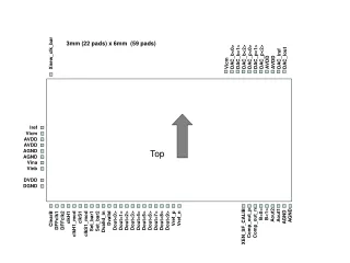
Vicm DAC_b<0> DAC_b<1> DAC_b<2> DAC_p<0> DAC_p<1> DAC_p<2> AVDD AVDD DAC_Iref DAC_Iout 3mm (22 pads) x 6mm (59 pads) Xnew_clk_bar Iref Vicm AVDD AVDD AGND AGND Vina Vinb DVDD DGND Top ClearB DFFclk1 DFFclk2 clkH1 clkH1_mod clkS1 clkS1_mod Set_bar1 Set_bar2 Dvalid_in Dvalid Dout<0> Dout<1> Dout<2> Dout<3> Dout<4> Dout<5> Dout<6> Dout<7> Dout<8> Dout<9> Vref_p Vref_n XEN_SF_CALIB Comp_out_p Comp_out_n B<0> B<1> Aout2 Aout1 AGND AGND
Vina and Vinb are sampled here 0 .1u.2u .3u.4u .5u .6u.7u .8u .9u1u 1.1u clkS1 set_bar1 DFFclk1 clkH1 set_bar2 DFFclk2 sample_in (adc valid) 1.2usec clock period The ADC clock is clkS1 ORed with clkH1 The DIO Board is based on a 10MHz clock (0.1usec clock period)
Digital Control Signals Vina and Vinb are sampled here 0 .1u.2u .3u.4u .5u .6u.7u .8u .9u1u 1.1u 1.2u clkS1 set_bar1 DFFclk1 clkH1 set_bar2 DFFclk2 sample_in (adc valid) One DAC Analog value 1.2usec clock period The ADC clock is clkS1 ORed with clkH1 The DIO Board is based on a 10MHz clock (0.1usec clock period)
ADC Control Signals overview 0 (1.2us) 2x(1.2us) 3x(1.2us) 4x(1.2us) 5x(1.2us) 6x(1.2us) Digital Control Signals Digital Control Signals Digital Control Signals Digital Control Signals Digital Control Signals Digital Control Signals DAC = 0 DAC = 1 DAC = 2 DAC = 3 DAC = 4 DAC = 5 Din<0> Din<1> Din<2> Din<3> Din<4> 1.2usec clock period
Design Number: 80172 Customer Name: Brita Olson Design Name: CPP2_ADC Customer Account: 3955 MOSIS PKG Name: PGA65 Phone: (909) 869-2652 Quantity Packaged: All Fax: (909) 869-4687 Min Pad Size (X): 78um Min Pad pitch (X): 90 um Min Pad Size (Y): 78um Min Pad pitch (Y): 90 um Cavity size: 400mils No Rotation Top