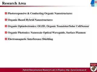
Research Area
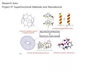
Research Area. Photoresponsive & Conducting Organic Nanostructures Organic-Based Hybrid Nanostructures Organic Optoelectronics: OLED, Organic Transistor/Solar Cell/Sensor Organic Photonics: Nanoscale Optical Waveguide, Surface Plasmon

Research Area
E N D
Presentation Transcript
Research Area Photoresponsive& Conducting Organic Nanostructures Organic-Based Hybrid Nanostructures Organic Optoelectronics: OLED, Organic Transistor/Solar Cell/Sensor Organic Photonics: Nanoscale Optical Waveguide, Surface Plasmon Electromagnetic Interference Shielding
Materials -Conjugated Polymers (Conducting Polymers): From insulating state to (semi)conducting state -Conjugated Molecules Alq3 rubrene pentacene perylene Graphene
Control tube or wire Diameter : 50 nm ~ 200 nm Length : up to 40 μm Conducting Polymer Nanotubes/Nanowires PEDOT Nanotube Nanoislands PPy Nanotube P3MT Nanotube PT Nanotube
Application Study for Conducting Polymer Nanotubes/Nanowires NanotipEmitter of Field Emission Display (FED) Single Strand Organic Transistor Source Gate Drain Transistor pattern Si3N4 or SiO2 Polypyrrole Nanotube or Nanowire Sample D (Au) S (Au) Insulator (Si3N4, SiO2) G (Au) Nanotip Emitter 3 ㎛ thickness ~ 2000Å
n S Organic-Inorganic, Organic-Organic Hybrid Nanostructure Bright Light Emission of PTh/metals Hybrid NTs • Charge Transfer Effect in SPR coupling • by using Doped-Polymer/Metal Hybrid NTs Simultaneous measurement PTh Cu PTh PTh/Cu 100 nm PTh/Cu PTh UV/Vis absorption spectra Cu ■ Doped-P3MT(0.67) NTs ●Doped-P3MT(0.52) NTs ▲Doped-P3MT(0.25) NTs ▼Doped-P3MT(0.04) NTs Diameter : ~ 200 nm Length : 40 m Wall thickness : 10 nm Cu 5 nm 100 nm • LCM PL intensity decreased with increasing doping level of P3MT NTs • LCM PL intensity increased with increasing doping level of P3MT/Ni HDLNTs • LCM PL intensity increased up to ~350 times • Enhancement of PL intensity(~100 times) through nanoscale metal coating on PTh NT due to surface plasmon resonance Ref.) J. Joo, D. H. Park et al., Adv. Mater. 19, 2824 (2007) Ref.) D. H. Park, J. Joo, et al., Adv. Func. Mater. 18, p.2526 (2008).
Organic-Inorganic, Organic-Organic Hybrid Nanostructure Light-Emitting MEH-PPV and MEH-PPV/Au Hybrid NPs Light-Emitting Color Barcode NWs (LECB-NWs) Reprecipitation Method • Alternating Electrochemical Polymerization Method • (P3BT-PEDOT NW compartments) • 22 NW compartments LCM PL spectra Au NPs Color CCD Au λex = 488 nm Au Au Au S S S Au Au MEH-PPV/Au single NP Au S S Au Au S S Au S Au MEH-PPV NP MEH-PPV single NP SEM Au Au Au Color CCD images LCM PL images LCM PL P3BT PEDOT MEH-PPV NPs MEH-PPV/Au NPs Ref.) M. S. Kim, J. Jooet al. ACS Nano 3, 1329(2009) Ref) D. H. Park, J. Joo, et al., ACS Nano,.4, 5155 (2010).
Organic Electronics : OLED Conventional OLED OLED using Nanomaterial Thin Film Deposition P3MT nanotubes : Lighting
Flexible OTFT Source Drain Gate 0V 18V 21V 23V 35V Organic Electronics : Organic Transistors Flexible and all-polymer based OTFT Conventional Organic Thin Film Transistor (OTFT)
Organic Optoelectronics : Photo responsive Organic FETs Highly photo-sensitive OTFT Memory operation with gate-field and light hν Erase Write 4(HPBT)-benzene 4(HP3T)-benzene Iph/Idark = 4×10³ ① ② ③ ④ Read (off) Read (on) D (Au) S (Au) On state TIPS-pentacene Active layer Insulator (SiO2) Gate (doped Si wafer) Off state • High reproducibility and retention ability (>1h) Photo-sensitivity (A/W) ΔId(≡ Id,ph−Id,dark ) /Pinc Memory operation processes: [writing-reading(on-state)-erasing-reading(off-state)]
Solar Cells • OPVCs using organic NPs enhancement of Light absorption Al electrode Organic NPs P3HT:PCBM PEDOT:PSS insulator ITO glass h • I-V characteristics and power conversion efficiency(PCE) curves • Control of PCE using diverse organic NPs
Focused Electron-Beam Treatment Schematic diagram of focused E-beam treatment Focused E-beam treated TiO2 NW 1.01018 1018 Color CCD images (ex = 405 nm) Focused E-beam Generator V E-beam source 5.01017 7.5 m 1017 1st Condenser lens 5.01018 5.0 m Aperture Length = 2.0 m Distance = 1.5 m 7.5 m 2nd Condenser lens Stigmator / Deflection coil 3-D LCM PL images (ex = 405 nm) 189 315 5.01017 Focused E-Beam ( ~ 100 nm) 1017 1018 99 7.5 m Pre-patterned Si wafer 5 m 10 m Focused E-beam treated organic/inorganic nanomaterials 5 m 5.01018
Focused E-beam treated P3MT NW 7.51016 electrons/cm2 I-V characteristic curves of P3MT single NW 2.51017 electrons/cm2 C O L O R C C D I M A G E Length : 0.25, 0.5, 1, 2 3, 4, 5, 6 m Length = 1 m Length : 0.5, 1, 2, 3, 4, 5 m • pristine Length = 2 m • single 5 m Au Au 100 nm • triple 3 D L C M P L I M A G E 130.5 1066.6 1.25 m Single junction P3MT NW Multi junction in the middle of NW (width/dosage = 100 nm/1.01017 electrons/cm2) Control of electrical properties 15 m 10 m 10 m 10 m
PMMA 1 m MWCNT MWCNT Composite for EMI Shielding PDP mesh filter for EMI Shielding Electromagnetic Interference Shielding EMI SE Measurement System EMI Shielding using Conducting Polymer
Characterization • Electrical Properties: • Temperature Dependent DC Conductivity (RTg10K) • Temperature Dependent AC Conductivity and Dielectric (RTg78K) • Microwave Conductivity and Dielectric Constant • I-V characteristics (with/without gate) • Photoresponsive I-V characteristics • Magnetic Properties: • EPR • SQUID • Magnetoresistance Optical Properties: • FT-IR Spectrum • UV/Vis/NIR Spectrum • Photo Luminescence • Laser Confocal Microscope Structural Properties • XRD • XPS • SEM, TEM
Research Equipment (1) DC Measurement System AC Measurement System • Temp. : 10 K ~ 350 K • DC Characteristics • I-V for Electronic Device • Temp. : 70 K ~ 450 K • Freq. : 10 Hz ~ 2 MHz • AC Characteristics
Research Equipment (2) Deposition Systems EMI SE Measurement System Organic Molecular Beam Deposition Thermal Evaporator
Research Equipment (3) Accessories Picoammeter and Sensitive Voltmeter Ball Bonder High Resolution Optical Microscope
Research Equipment (4) LCM PL Measurement Glove Box