1.74A to 2.33A
70 likes | 138 Vues
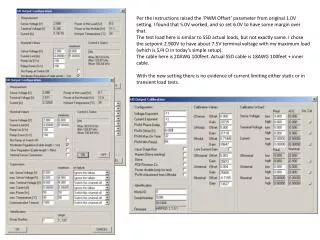
Per the instructions raised the ‘PWM Offset’ parameter from original 1.0V setting. I found that 5.0V worked, and so set 6.0V to have some margin over that.

1.74A to 2.33A
E N D
Presentation Transcript
Per the instructions raised the ‘PWM Offset’ parameter from original 1.0V setting. I found that 5.0V worked, and so set 6.0V to have some margin over that. The test load here is similar to SSD actual loads, but not exactly same. I chose the setpoint 2.900V to have about 7.5V terminal voltage with my maximum load (which is 5/4 Ωin today’s simple setup). The cable here is 20AWG 100feet. Actual SSD cable is 18AWG 100feet + inner cable. With the new setting there is no evidence of current limiting either static or in transient load tests.
Load capacitance: 2x470uF (TAJD477K006RNJ) Load switched mechanically by tapping on/off the 4th resistor lead. Some glitches probably occur in this process, I generally rejected and retook measurements that were obviously glitchy. 2.33A to 1.74A 1.74A to 2.33A
2.33A to 1.74A 1.74A to 2.33A Load capacitance: 1x470uF (TAJD477K006RNJ)
Load capacitance: ~10uF Y5V ceramic NOTE SCALE CHANGE 2.33A to 1.74A 1.74A to 2.33A
Load capacitance: NONE 2.33A to 1.74A 1.74A to 2.33A
Summary is that it is stable under all those conditions and no current limiting is seen in the transient response. All good! The SSD group internally needs to quantify what transient loads will actually be expected, and then evaluate if the resulting voltage excursions are tolerable. If not, then point-of-load regulation needs to be added/modified. I believe the response we see from this power supply on 100 feet cable is reasonably optimal, no complaints. All this focussed on the “medium” loop gain control setting. I did confirm that “fast” control is unstable (as advertised/expected), and that “slow” is a real extreme slow loop and of no utility with any transient load situation.
Ripple/noise: Nothing detectable at load with simple measurement (500MHz BW, P6139A 10x atten. probe). Good. At load At PS terminals