Download
1 / 23
230 likes | 381 Vues
The Pad HPD as Photodetector of the LHCb RICH Detectors. C. Joram for the Pad HPD team. General Design L0 Electronics R&D: Results + Future Tube Fabrication + costs. High sensitivity for E<5.5 eV. Large area. Granularity ca. 2.5 mm. High filling factor.

E N D
The Pad HPD as Photodetector of the LHCb RICH Detectors C. Joram for the Pad HPD team • General Design • L0 Electronics • R&D: Results + Future • Tube Fabrication + costs
High sensitivity for E<5.5 eV Large area Granularity ca. 2.5 mm High filling factor Single photon sensitivity Robust operation Cost effectiveness LHC speed readout LHCb RICH Requirements
The Design of the Pad HPD • Total (active) diameter: 127 (114) mm 69% filling factor when hex. closed pack + 3mm gap space for mu-metal + insulation • Bialkali photocathode + UV extended borosilicate window good compromise between DE and sqchrom. • Fountain shaped electron optics purely linear adjustable demagnification strong E-field over full tube robustness against magnetic fields • Work at maximum high voltage (25 kV) large signal (ca. 6000-6500 e-) low point spread function (pixel error) robustness against magnetic fields • Round Si sensor with pads of 1 x 1 mm2 no dead space, no unused pads pixel error matches other error sources n E
Analog readout electronics full exploitation of information continuous online pedestal determination + subtraction can cope with common mode + other noise sources • Tube design allows to re-use all components • Tube can be manufactured by LHCb RICH group or by industry
L0 Electronics of the Pad HPD • SCTA128 modified according to LHCb specifications. • SCTA128_LHCb • Analog readout chip in rad hard DMILL technology. • Chip is fully identical with proposed mvtx chip. • SCTA128 exists and has demonstrated • peaking time 25 ns • analog multiplexing at 40 MHz • expected noise figures: 398 + 55 pF-1 • For the Pad HPD (ca. 4 pF) we expect a pedestal noise of 650e- ENC S/N = 10 det. = 92.8% (4s cut) • Necessary LHCb modifications will be discussed • under future R&D
R&D programme of the Pad HPD Concept, design, fabrication of HPD components Test of electron optics, Si sensor, VA electronics (CsI PC) Design, fabrication, commissioning of HPD plant Development of tube processing (PC, sealing, getter) Further optimization of processing. Final electronics. • Main Results of the R&D • Difficulties and problems • Future R&D
Main Results of the R&D • Quantum efficiency of bialkali cathodes Q.E. of a good HPD Summary of all cathodes produced since March 1999
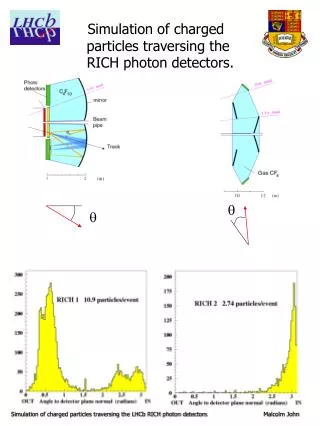
Comparison of lab. measured Q.E. • and test beam data • PC59 tested with 180 cm long C4F10 radiator • Expect 48 p.e. • Find 54 p.e. (noise subtracted) • Agreement • within • uncertainties Online display of single event ring • Electron Optics of the Pad HPD • 114 mm active • Linear demagnification, • adjustable • Fit residuals 200 mm
Electron optics with mu-metal shield 128 mm, 0.9 mm thick Linear optics not affected by grounded shield.
Point spread function measured on Si plane
Measurement in B-field (Helmholtz coil) Axial B-field, no shield Axial B-field, with shield
Transverse B-field, y measured on Si-plane x B • A 160 mm long mu-metal shield is very effective for • BE : reduction of DF by factor 12, DR/R0 • BE: reduction of Dx by factor 12 • For reasonably low fields (B<10 Gauss) the shift and the rotation becomes negligible • A short shield (110 mm) has been tested but found to • be less efficient (only factor 3 reduction) • If a long shield has to be used, a pointing geometry is possible (12% fewer tubes required) For reasonably low fields (B<10 Gauss) the shift and the rotation become negligible pointing geometry
1 p.e. Viking VA3 chip (tpeak = 1.3 ms, 300 e- ENC) UC = -26 kV 2 p.e. Single pad S/N = 20 3 p.e. • Signals on the Si sensor Pedestal cut (4s) ADC counts thanks to a thinned n+ and Al layer
Exposure to direct charged particles • Data at 0º and 25º incidence angle • Photons from C-effect in window well • localized 20-40 multi photon hits. • Charged particles in Si sensor easily identifiable • Results in agreement with Malcolm’s simulations. • Analog information useful for event cleaning. C-photons from window sx =sx 1.2 mm Signals from charged particles sx 1.3 mm sY 2.2 mm
Difficulties and Problems • Phototube fabrication is not extremely difficult, but... • we started essentially from zero • many parameters have to be precisely tuned • difficult diagnostics of ambiguous symptoms • only few trials Two problems caused significant delays • Some envelopes develop leaks during bakeout Problem understood and fixed by SVT. A good fraction of our envelopes are affected. However: All tubes can be repaired! • Some tubes with bialkali cathode do not stand full cathode voltage Problem understood but not fully fixed. K and Cs atoms adhere to impurities on glass surface. Surface conductivity Field distortions atomic excitation under HV light emission Improved (chemical) cleaning helps ! Walls can be protected by mask. To be tested.
Future R&D • Further optimization and stabilization of the of tube fabrication process • Build tubes with final LHCb electronics • Modification of SCTA • analog frontend • FE identical to existing ABCD chip • expect 650 e- noise in Pad HPD • submission still in 1999 • Modifications of SCTA • backend • 4 ms pipeline • 432 multiplexing • reduced set-up time • submission by 2/2000
In the meantime… • demonstrate vacuum operation of existing SCTA128HC • demonstrate baking of SCTA128HC • Finally… • produce sealed HPD with existing SCTA128HC • produce sealed HPD with final SCTA128_LHCb R&D finished by mid 2000 !
Tube Fabrication We considered 3 possible fabrication scenarios A) In-house production at CERN (baseline of proposal) B) Distributed in-house production (CERN + other institutes inside LHCb) c) Industrial fabrication: 1 offer available (Thomson, France), a 2nd offer in preparation (Photek, UK)
Our baseline scenario 240 Pad HPDs are required to be ready and tested by mid 2004. 2 new optimized fabrication plants have to be built (re-using existing special components) 4 Pad HPDs are produced per week 240 tubes can be produced in 22 months assuming average yield of 80% 40 production weeks/yr HPD fabrication should start by beginning of 2002 • There is sufficient time to • design, build and commission plants • re-iterate on SCTA128 if required All technical labour is included in cost estimate !
Cost estimate (Details will be given by Dave Websdale.) Total cost of 216 tubes (incl. encapsulated electronics) A) In-house: 2.0 MCHF (ca. 30% labour) B) Distr. in-house: unknown, could be less than A) C) Industry: 3.2 MCHF
Conclusion • The Pad HPD is a photodetector which has been coherently designed to fulfill the LHCb RICH requirements in an optimum way. • The achieved performance and the expected results of the remaining R&D phase make it an excellent candidate. • The (distributed) in-house fabrication represents a cost-effective scenario, which allows to produce all tubes well in time and still provides sufficient reserves. Many thanks to all members of the Pad HPD team, our industrial partners, and all people who generously supported us.