X-ray Spectroscopy in SEM and TEM: Understanding Braking and Elemental X-ray Peaks
Learn about the emission of X-rays during braking in scanning electron microscopy (SEM) and transmission electron microscopy (TEM). Understand how atomic properties impact characteristic X-ray production, and explore the use of silicon detectors in X-ray energy dispersive spectroscopy (EDS).

X-ray Spectroscopy in SEM and TEM: Understanding Braking and Elemental X-ray Peaks
E N D
Presentation Transcript
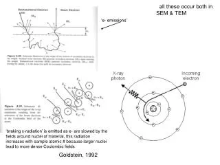
all these occur both in SEM & TEM ‘e- emissions’ ‘braking x-radiation’ is emitted as e- are slowed by the fields around nuclei of material, this radiation increases with sample atomic # because larger nuclei lead to more dense Coulombic fields Goldstein, 1992
Characteristic x-ray production is defined by atomic orbital e- transitions EKα = EK – EL Ekβ = EK-EM so EKα<Ekβ<EK<E beam e- EK or EM here is ionization energy, the energy difference between these = the observed x-ray energies Y axis is # of xray photons Each of these lines can correspond to a peak in a spectrum like the one at left X axis is energy of xray photons characteristic (elemental) x-ray peaks braking radiation Goldstein, 1992 Can we can do x-ray spectroscopy in SEM? How about optical confocal microscope?
e- beam Intrinsic region is also here after Li drifting during manufacture 2D sample Cross sectional diagrams of silicon [Si(Li)] x-ray detector used in x-ray eds. These diagrams show two slightly different views. The intrinsic region of each detector is Li doped and is the region that counts x-rays by converting their energy into electron current. Normal P (boron doped) or N (phosphorus doped) type silicon is not a good x-ray detector because of excessive e- and hole current even in the absence of an x-ray event. e- beam 3D X-rays The next 2 slides address spectral artifacts and how the EDS detector disperses the xray energies for plotting. sample
You will not be tested on this page but it may help you with other concepts. The Si detector and the escape peak: When an x-ray enters detector, it makes a charge pulse that is monitored. This pulse has size (total # of e- counts in detector) based on the formula: # of e- counts = Energyx-ray in eV/ ε’ (ε’ = 3.8 eV for Si, this is the energy needed to create an e-/hole pair in our detector, notice how low this value is, it must be a bonding (molecular) e-, not an inner shell e- that is involved) Usually, this energy is entirely captured by multiple electronic/kinetic events inside the detector. If it is not, say an inner shell Si electron is displaced and a Si K x-ray (1.74 keV) is generated and escapes, now the pulse count does not accurately represent the energy of the incoming x-ray as some energy has escaped. This event causes us to see the ‘escape peak’ which is seen on our spectrum at 1.74 keV below the actual incident x-ray energy peak of the sample.8.04keV (Cu K) – 1.74keV (Si K) = 6.3keV (Cu K escape peak)
Top and bottom spectra are the same data, just different scaling. The electron beam was focused on the sem specimen stage which is made of a brass alloy; mostly copper and zinc. Although these spectra show system peaks by definition (these are x-rays coming from part of our microscope chamber or the stage) we do not call them artifacts because we were intentionally focused and collecting signal from our sem stage. In this case, our system is our sample! main Cu K peak (Kα) at 8.04 keV main Cu K peak (Kα) at 8.04 keV ? Cu Kα escape peak Cu Kα escape peak Cu Kα sum peak Low beam current (30% dead time on detector) High beam current (60% dead time) Why does too much beam current lead to this copper ‘sum peak’ (far right arrow)? What is the apparent benefit of the higher beam current setting? Can you find the Cu escape peak? See lower right spectrum and look down energy from the very large Cu peak.