Download

1 / 101
1.02k likes | 1.17k Vues
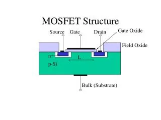
CMOS MOSFET problems. Complementary MOS inverter “CMOS” inverter. Complementary MOS inverter “CMOS” inverter. n channel enhancement mode ( V tN > 0) in series with a p channel enhancement mode ( V tP < 0)

E N D
CMOS MOSFET problems
ComplementaryMOS inverter“CMOS” inverter • n channel enhancement mode (VtN > 0) in series with a p channel enhancement mode (VtP< 0) • 0 < Vin< VTn--NMOS drain current is zero PMOS drain current will also be zero. • Vsgp=Vdd– Vin Vdd > |Vtp| • Therefore, in order to have no current, VSDp = 0 or Vout = Vdd
ComplementaryMOS inverter“CMOS” inverter • n channel enhancement mode (VtN > 0) in series with a p channel enhancement mode (VtP< 0) • Vdd - |Vtp|< Vi < Vdd– PMOS drain current is zero & NMOS drain current will also be zero. • Vsgn= Vin Vdd > Vtn • Therefore, in order to have no current, Vsdn = 0 or Vout = 0
Important changes in the MOSFET Moore’s Law (Intel Corp. cofounder) The number of active elements on a chip doubles every 18 months.
Important changes in the MOSFET constant electric field!
Important changes in the MOSFET Material determination weak dependence on k
Problem in changing the MOSFET We will not change our old power supplies. Do not, I repeat, do not change the voltage supplies so often. • Consequences • electric fields increase in value. • 2) reduced reliability. • 3) heating
V G Depletion layer expansion in the MOSFET Long channel Space charge regions Flatband "Punch through"
Energy level diagrams before and after “punch through” After Before
E V G “hot electrons” MOSFET The drain-source voltage increases causing impact ionization at the drain electrode. The depletion layer increases Electrons go into the oxide region and the holes going to the substrate. Hot electron energy > Thermal equilibrium value Electrons may “tunnel” into the oxide
E Lightly doped MOSFET
Transmission line modeling simulation with PSpice ASEE conference 2007
Transmission Lines Demonstration High Frequency Electronics Course EE527 Andrew Rusek Oakland University Winter 2007 Demonstration is based on the materials collected from measurement set up to show sinusoidal and step responses of a transmission line with various terminations. Results of selected simulations are included.
Fig. 1b Low frequency sine-wave (1MHz), TL matched (50 ohms), observe small delays and almost identical amplitudes
Fig. 1c Low frequency sine-wave (1MHz), TL matched (50 ohms) Channel 4 (output) shows the voltage for grounded center conductor and a probe input connected to the outer conductor (shield), observe the phase inversion of the last wave (180 degrees)
Fig. 2a Sine-wave of 17 MHz, matched load The waves have the same amplitudes, the phases are different.
Fig. 2b Sine-wave of 17 MHz, matched load Channel 4 (output) shows the voltage for grounded center conductor and a probe input connected to the outer conductor (shield).
Fig. 3 Open ended TL, sine-wave of 1 MHz applied, observe 2X larger amplitude in comparison with previous tests, amplitudes are almost the same for all waves.
Fig. 4a Open ended TL, 3.5 MHz, observe minimum (input) One quarter wave pattern is shown
Fig. 4b Open ended TL, 3.5 MHz, observe minimum (input) One quarter wave pattern is shown
Fig. 4c Open ended TL, 3.5 MHz, observe minimum (input) One quarter wave pattern is shown
Fig. 5 Open ended TL, 5.5 MHz, observe shift of the minimum The minimum is located quarter wave from the end.
Fig. 7 Shorted TL, low frequency,1MHz applied, observe zero output voltage
Fig. 9 Shorted TL, 7 MHz, observe two minima (half wave). If the length of the line is known, the dielectric constant can be calculated (Lambda_cable/2 = 12m, open space Lambda = 42.8m).
Fig. 10 Shorted TL, 7 MHz, increased vertical sensitivity; observe two minima as before and effects of stray inductance of the source and probe leads (half wave),
Fig.11 Shorted TL, 11 MHz, two minima, first shifted towards the load, ¼ wavelength + ½ wavelength
Fig. 12 Pulse response of open ended TL, slow pulse (0.3us rise time), no reflections observed, Channel 2 – Input, Channel 4 – Output, observe the delay.
Fig. 13a Open ended TL, Input Pulse rise time = 240 ns, Output = 120 ns, Long pulse applied, measurement circuit
Fig. 13b Open ended TL, Input Pulse rise time = 240 ns, Output = 120 ns, Why Output is faster than Input ? End of TL reflection adds to incident (Real rise time of the input wave is120 ns), and this effect doubles Input signal rise time. Long pulse applied, simulations.
Fig. 13c Open ended TL, Input Pulse rise time = 240 ns, Output = 120 ns, Why Output is faster than Input ? End of TL reflection adds to incident (Real rise time of the input wave is120 ns), and this effect doubles Input signal rise time. Long pulse applied, measurements.
Fig. 14a Open ended TL, long pulse applied, source matched, measurement circuit.
Fig. 14b Open ended TL, long pulse applied, source matched, simulations.
Fig. 14c Open ended TL, Input – Channel 2 shows incident step and reflected step (doubled TL delay), source matched, Output – Channel 4 shows doubled incident wave level, delayed (about 60 ns), long pulse applied. Distance between steps of Channel 2 – 2X TL delay time, measurements.
Fig. 15c Open ended TL, short pulses applied to show “radar effect”, circuit.
Fig. 15c Open ended TL, short pulses applied to show “radar effect”. Echo is observed (Upper Channel – Input), doubled amplitude – Lower Channel, simulations.
Fig. 15c Open ended TL, short pulses applied to show “radar effect”. Echo is observed (Channel 2 – Input), doubled amplitude – Channel 4 – Output, observe effects of the losses of TL – echo is slower and smaller. Distance between pulses of Channel 2 – 2X TL delay time. Measured unit delay yields 20cm/ns.
Fig 16b Shorted TL, narrow pulses, observe change of polarity of a reflected pulse (Upper Channel – Input).