Download
1 / 22
220 likes | 454 Vues
Carbon Nanotubes of DNA. EE 240 Project May 1, 2007. By: Amit Dewan Justin Keeney Sahil Ashok Deora. Group 7. Carbon Nanotubes. What are they?

E N D
Carbon Nanotubesof DNA EE 240 Project May 1, 2007 By: Amit Dewan Justin Keeney Sahil Ashok Deora Group 7
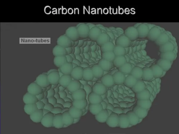
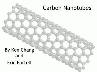
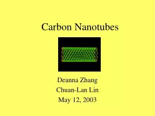
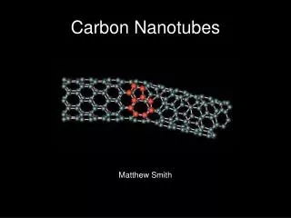
Carbon Nanotubes • What are they? • They are single sheet of carbon atoms rolled together. They are very small objects and exhibit many different structures and properties. • There are 4 different types of carbon nanotubes. • Single walled - one atom thick layer of graphite. • Multi walled – multiple layers of graphite. • Fullerite- solid state manifestation of fullerenes. • Torus – donut shaped.
DNA • Deoxyribonucleic acid • DNA is a long polymer of simple units called nucleotides, which are held together by a backbone made of sugars and phosphate groups.
Its Applications • The combination of their electronic properties and dimensions makes carbon nanotubes ideal building blocks for molecular electronics. • The advancement of carbon nanotube is based on the electronics required for assembly strategies that allow the precise localization and interconnection. Using the method of recognition between molecular building blocks, we can realize the self-assembled carbon nanotube field-effect transistor operating at room temperature. A DNA scaffold molecule provides the address for precise localization of a semiconducting single-wall carbon nanotube and where the extended metallic wires contacting it are placed.
SWNT - FET • Individual single-wall carbon nanotubes (SWNT) have been used to realize molecular-scale electronic devices such as single-electron and field-effect transistors (FET). • Several SWNT-based devices have been successfully integrated into logic circuits and transistor arrays
Assembly of a DNA-templated FET and wires contacting it. The following steps are: (i) RecA monomers polymerize on a ssDNA molecule to form a nucleoprotein filament. (ii) Homologous recombination reaction leads to binding of the nucleoprotein filament at the desired address on an aldehyde-derivatized scaffold dsDNA molecule. (iii) The DNA-bound RecA is used to localize a streptavidin-functionalized SWNT, utilizing a primary antibody to RecA and a biotin-conjugated secondary antibody. (iv) Incubation in an AgNO3 solution leads to the formation of silver clusters on the segments that are unprotected by RecA. (v) Electroless gold deposition, using the silver clusters as nucleation centers, results in the formation of two DNA-templated gold wires contacting the SWNT bound at the gap
Formation of SWNT FETwith DNA – Step 1 • The SWNT-FET is assembled via a three-strand homologous recombination reaction between a long double-stranded DNA (dsDNA) molecule serving as a short, auxiliary single-stranded DNA (ssDNA) • The short ssDNA molecule is synthesized so that its sequence is identical to the dsDNA at the designated location of the FET • RecA proteins are first polymerized on the auxiliary ssDNA molecules to form nucleoprotein filaments which were then mixed with the scaffold dsDNA molecules
Formation of SWNT FETwith DNA – Step 2 • A nucleoprotein filament bound a dsDNA molecule according to the sequence homology between the ssDNA and the designated address on the dsDNA • The RecA later helped localize a SWNT at that address and protect the covered DNA segment against metallization
Formation of SWNT FETwith DNA – Step 3 • Streptavidin-functionalized SWNT was guided to the right location on the scaffold dsDNA molecule using antibodies to the bound RecA and biotin-streptavidin–specific binding and the SWNTs were solubilized in water by micellization in SDS • Streptavidin is a tetrameric protein purified from Streptomyces avidinii that binds very tightly to the vitamin biotin. The strong streptavidin-biotin bond can be used to "glue" various chemicals onto surfaces
Formation of SWNT FETwith DNA – Step 3 • antibodies to RecA were reacted with the product of the homologous recombination reaction, resulting in specific binding of the antibodies to the RecA nucleoprotein filament • Next, biotin-conjugated secondary antibodies, which have high affinity to the primary ones, were localized on the primary antibodies to RecA • Finally, the streptavidin-coated SWNTs were added, leading to their localization on the RecA via biotin-streptavidin–specific binding
Localization of a SWNT at a specific address on the scaffold dsDNA molecule using RecA. (A) An AFM image of a 500-base-long ( 250 nm) RecA nucleoprotein filament (black arrow) localized at a homologous sequence on a = DNA scaffold molecule. Bar, 200 nm. (B) An AFM image of a streptavidin-coated SWNT (white arrow) bound to a 500-base-long nucleoprotein filament localized on a -DNA scaffold molecule. Bar, 300 nm. (C) A scanning conductance image of the same region as in (B). The conductive SWNT (white arrow) yields a considerable signal whereas the insulating DNA is hardly resolved. Bar, 300 nm
Formation of SWNT FETwith DNA – Step 4 • After stretching on the substrate, the scaffold DNA molecule is metallized. The RecA, doubling as a sequence-specific resist, protects the active area of the transistor against metallization. • Aldehyde residues, acting as reducing agents, are bound to the scaffold DNA molecules by reacting the latter with glutaraldehyde (is also used for industrial water treatment and as a chemical preservative). • Highly conductive metallic wires were formed by silver reduction along the exposed parts of the aldehydederivatized DNA
Formation of SWNT FETwith DNA – Step 5 • subsequent electroless gold plating using the silver clusters as nucleation centers • Because the SWNT is longer than the gap dictated by the RecA, the deposited metal covers the ends of the nanotube and makes contact with it .
A DNA-templated carbon nanotube FET and metallic wires contacting it. SEM images of SWNTs contacted by self-assembled DNA-templated gold wires. (A) An individual SWNT. (B) A rope of SWNTs. Bars, 100 nm
Its Properties • The DNA-templated gold wires are contacted by e-beam lithography, and the device is characterized by direct electrical measurements under ambient conditions. • The gating polarity indicates p-type conduction of the SWNT, as is usually the case with semiconducting carbon nanotubes in air. • The saturation of the drain-source current for negative gate voltages indicates resistance in series with the SWNT. The resistance is attributed to the contacts between the gold wires and the SWNT because the resistance of the DNA-templated gold wires is typically smaller than 100 ohms.
Electrical characteristics of the DNA-templated carbon nanotube FET. (A) Schematic representation of the electrical measurement circuit. (B) Drain-source current (IDS) versus drain-source bias (VDS) for different values of gate bias (VG). VG = –20 V (black), –15 V (red), –10 V (green), –5 V (blue), 0 V (cyan), 5 V (magenta), 10 V (yellow), 15 V (olive), 20 V (slate blue). (C) Drain-source current versus gate voltage for different values of drain-source bias [same device as (B)]. VDS = 0.5 V (black), 1 V (red), 1.5 V (green), 2 V (blue).
Properties – contd. • The rope devices cannot be turned off by gate voltage, probably due to the fact that they contain metallic nanotubes in parallel with the semi-conducting ones • The metallic nanotubes cannot be depleted by the available electric field. As the gate bias is made more positive, the rope conduction decreases but saturates to a finite value. • Different devices have somewhat different turn-off voltages. They all exhibit hysteresis in the drain-source current as a function of gate bias
Advantages • The realization of a SWNT FET in a test tube promotes self-assembly as a realistic strategy for the construction of carbon nanotube-based electronics. The approach developed here can be generalized, in principle, to form a functional circuit on a scaffold DNA network. • Numerous molecular devices could be localized simultaneously at different addresses on the network and interconnected by DNA-templated wires. • The RecA-based scheme is robust and general enough to allow flexibility in the integration of other active electronic components into circuits. • Realization of a functional circuit will require improving the electronic properties of the transistor and individual gating to each device. The latter could be achieved by using a three-armed DNA junction as a template with the SWNT localized at the junction and by developing a method for turning one of the arms into a gate.
DIFFICULTIES • the difficulty in precise localization and interconnection of nanotubes impedes further progress toward larger-scale integrated circuits. • The process should carried at temperature below the melting temperature of DNA.
References • http://en.wikipedia.org/wiki/Main_Page • http://ieeexplore.ieee.org • http://www.news.uiuc.edu/NEWS/06/0126nanotubes.html • http://www.sciencemag.org • http://www.rsc.org/ej/OB/2004/b402044h.pdf • http://www.hindu.com/seta/2003/12/18/stories/2003121800391800.htm • http://arjournals.annualreviews.org • http://pubs.acs.org/cen/news/83/i23/8323notw8.html
THANK YOU!!!!!!!!!!!!!! ENJOY THE FREE FOOD