Ion Implantation
Ion Implantation. Topics: Deposition methods Implant -Depth & Distribution -Masking effects Damage annealing . Manufacturing Methods. Applying a magnetic induction, B, to speeding atoms causes them to bend around the curve of radius R: ½ mv 2 = q . v x B

Ion Implantation
E N D
Presentation Transcript
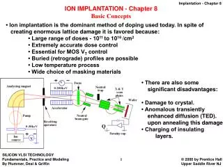
Ion Implantation • Topics: • Deposition methods • Implant • -Depth & Distribution • -Masking effects • Damage annealing
Manufacturing Methods Applying a magnetic induction, B, to speeding atoms causes them to bend around the curve of radius R: ½ mv2 = q.v x B Velocity can be expressed as: v = √(2E/m) = √(2qVext/m) B can be expressed as a function of current: B = aI Thus √m = q/√2E(aR)I By adjusting current, I, ions can be separated by mass Schematic of an ion implanter Ion source: Vaporized solids or gases – e.g., - - Arsine - Phosphine - BF2 These gases are extremely toxic! Mixed in 15% concentrations with H2 Vapors form various species, such as B++, B+, BF+, BF2+, along with neutral atoms
Neutrals are separated by the electrostatic deviation of the focus beam Ions are precisely counted using a “Faraday cup”
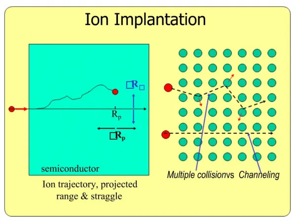
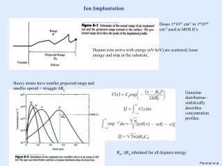
Ion Path and Distribution Schematic of the actual range of an implanted ion and the projected range normal to the surface. Distribution of ions implanted into crystalline silicon at an energy of 200 keV. Light ions penetrate more deeply, and have more asymmetric distribution than heavy ions. Definitions: Cp = peak concentration Rp = average projected depth DRp = Standard Deviation =
Dopant concentration curves are modeled using Gaussian distribution: Total number of ions implanted: This relates the dose to the peak concentration Plots of Rp and DRp for common dopants in crystalline Si tilted and rotated to simulate random direction.
Lateral distributions are also modeled using a Gaussian: Simulated 3D distribution of 1000 P atoms implanted at 35 keV (top). Axis units are nm.
Masking Layers Solving for xm: Schematic of masking process, where dose Qp penetrates the mask of thickness xm. * denotes mask The dose that penetrates is:
Implantation not Perpendicular to Mask The dopant distribution resulting from tilt implantation followed by diffusion is given by combining implantation concentration and diffusion equations: Implantation Simulation of 50 keV P implant at a tilt angle of 30o, showing asymmetrical implant distribution and shadowing caused by the gate polysilicon Diffusion
Actual distributions Simulated profiles of B implanted in amorphous or polycrystalline Si over a range of energies. Profiles show noticeable skew toward surface due to backscattering of light B ions. Skewed profiles are described by a 4-factor Pearson distribution. Gaussian fit to 500 keV profile is shown by dashed line. Evolution of Gaussian profile after annealing. The Gaussian preserves its shape as it diffuses in an infinite medium.
To accurately model, we need to include 4 parameters: • Projected range, Rp • Scatter, DRp • “Skewness” due to mass effects, g • Kurtusis, or variation due to occasional extremes, b • Thus • f(curve) = f(Rp, DRp, g, b) Simulation of ion-implanted B and Sb profiles with implant energy adjusted to give the same range. Light B ion skews toward surface, while heavy antimony ion skews toward bulk.
The role of crystal structure Ions undergo many small angle deflections when traveling in a channel Clockwise from top left: Image of a silicon crystal looking down the 110 axial channels, the 111 planar channels, the 100 axial channels, and with tilt and rotation to simulate a “random” direction Simulated boron profiles implanted into <100> Si wafers with zero tilt & rotation.
Implantation Damage & Annealing Goal: to remove damage from implantation and return Si to a crystalline state leaving dopants in substitutional sites. Simulation of recombination of vacancy (V) and interstitial (I) damage resulting from implantation. At 800 oC, recombination takes place very quickly. After a short time, only excess interstitial clusters remain Si interstitials condense into ribbons of Si atoms (I-dimers) lying on {311} planes and grow by extending in the <110> directions. On right is a TEM image of clusters
At high temperatures, ribbons condense and grow, creating dislocation loops that populate the boundary between crystalline and amorphous silicon. TEM of EOR dislocation loops for annealing times of 5, 60 and 960 minutes at 850 oC (a-c), and for 1, 60 and 400 sec. at 1000 oC (d-f). Loops show some ripening (large loops grow at the expense of small loops) but are very stable at typical annealing temperatures. Schematic of stable End-of-Range (EOR) dislocation loops that form at amorphous/crystalline interface