PT module design and readout
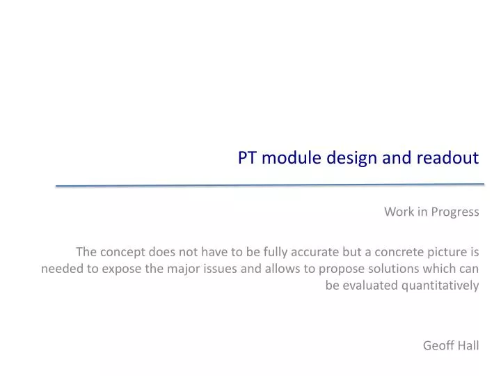
PT module design and readout. Work in Progress The concept does not have to be fully accurate but a concrete picture is needed to expose the major issues and allows to propose solutions which can be evaluated quantitatively Geoff Hall. Overall layout [Mark P].

PT module design and readout
E N D
Presentation Transcript
PT module design and readout Work in Progress The concept does not have to be fully accurate but a concrete picture is needed to expose the major issues and allows to propose solutions which can be evaluated quantitatively Geoff Hall
Overall layout [Mark P] • Assume stacked layer at R ≈ 25 cm • Tilted to minimise cluster size • large clusters from grazing incidence • need to simulate low pT tracks • efficiency bias for oppositely charged low pT tracks? relevant if full readout for tracking is used? R = 25cm thickness = 285µm G Hall
Occupancy estimates • Scenarios for sLHC and vLHC W Scandale & F Zimmerman • Nuclear Physics B (Proc. Suppl.) 177–178 (2008) 207–211 • 40MHz, peak luminosity 1.55x1035 • <294 interactions/bx> • PYTHIA & total sinelastic(pp) = 79mb -> <306 interactions/bx> • Then geometry dependent • R = 25cm |h|=2.5, untilted sensors, 100um x 2.5mm pixels • average occupancy over layer is 0.45% ± 17%[3s Poisson variation], • cross section uncertainty = ±30%[Tomalin], low pt track uncertainty = ±12%[Tomalin], cluster width uncertainty = ±50%[simulation] => (0.45 ± 0.3)% occupancy. • Other factors include fluctuations in jets – being studied G Hall
PT layer pixel size • Should reduce need to compare many nearby columns • D independent of h, but offset in z between layers increases with h • R-f: compare to assembly precision ~ 100µm R = 25cm, L =28cm d = 2mm ∆ ≈ 2 mm ∆ ∆ d d ∆ = dL/R R R q q’ Luminous region L L LHC luminous region L ≈ 28cm (±3s) – may be larger or smaller at SLHC G Hall
Schematic PT module Correlator R = 25cm Occupancy ~ 0.5% at 40MHz & 1035 -This is believed to be worst case Data out 104 x 2 128 x100µm x 2x2.5mm 12.8mm data 2 x 2.5mm Inexpensive prototyping, using wire bonding, might be possible - experimental demonstration will be important G Hall
PT layer readout column of 128 pixels • Bring data for comparison with second layer, using minimum power • high speed shift register? 128/25ns = 5.12Gb/s • try to exploit low occupancy? • address hit channels? • 128 = 7 bits • and should handle some multiple hits • high PT candidates should be narrow clusters • ignore clusters of 3 or more strips • likely to be only one candidate group per 128 channel even in congested environment G Hall
Possible schematic column of 128 pixels • divide column into 32 x 4 channel groups • eg logic sets 9 address lines: • 5 bit group + 4 bit pattern +1 bit spare • provide more information than single channel address • ignore combinations consistent with wide clusters • a moderate number of address lines could be sufficient • still plenty of space for power, clock, I2C, … • probably share some in 256 channel chip • Nearest neighbour logic to avoid group boundaries • including (upper) chip edge G Hall
Some details column of 128 pixels • Valid 4 bit patterns • 0001 0010 0100 1000 … 0011 0110 1100 … • 1011 1101 = double cluster • Invalid • 0000 1111 1110 0111 • Although infrequent, there will be adjacent groups – nearest neighbour logic to merge • eg is an invalid cluster • Could also increase address lines to cope • eg 110 groups of 8 channel groups => 12 bits • cf 32 groups of 4 channels => 10 bits • Optimise design using MC • eg 256 elements, longer groups, and to avoid bias G Hall
More details • At central boundary need data from ROC-L & ROC-R • extra level of bonding? [pixel:127] [pixel:0] ROC-L ROC-R ROC-L ROC-R Simplest solution: If a valid pattern with hit in [pixel:127] pass all data from last pixel, even if match not found use spare bit as indicator that no matching comparison extra data volume, for rejection factor 20 (1 + 127*0.05)/(128*0.05) ≈ 1.15 G Hall
Data rate for PT module Correlator Module 25.6mm x 80mm 256 x 32 sub-units = 8192 channels Occupancy ~ 0.5% => 40 hit channels PT reduction ≈ 20 [Mark P] => 2 hit channels/BX ≈ 32 bits, with column address Data out 104 x 2 128 x100µm x 2x2.5mm 12.8mm data 2 x 2.5mm G Hall
ROC Height: 128 x 100µm = 12.8mm +… Width: 2 x 1.5mm = 3mm + Space for bond pads, etc…. Dense bonds on module : 8192 channels Optimised pitch size? Max chip size in 130nm: 19.5mm x 21mm Functions: amplifier, threshold adjustment, comparator, latch, neighbour logic, connect to bus, internal test? Questions could assembly be done using inexpensive bump bonding? eg C4 layout with 200µm spacing should be possible Power transmission over long, narrow chip? ROC-2: 128 chan ROC-1: 128 chan G Hall
Module - plan view of section upper layer lower layer column 128 channels column 128 channels 10 bit bus 10 bit bus assembler 10 bits from column above transmits column to each neighbour receives 10 inputs from each neighbour and stores receives 10 inputs from module below compares pattern from module below with three (10 bit) stored patterns assembler x10 x10 x10 x10 store + (memory buffer for full readout) x10 x10 x10 x10 x10 x10 x10 x10 x10 x10 interconnect chip multi-via G Hall
Module - section view in r-f plane assembler ROC PCB 2mm sensor store ROC PCB Interconnect chip mass produced, cheap coarse pitch ~250µm ~2.5mm x 2.5mm Maybe an easier method? Sensor & ROC ~ 200µm thick Very small component, with regular spacing -… G Hall
Possible connectors O Zorba Fine Stack .40 mm Pitch Plug & Receptacle Number of Positions = 80 (also 20,24,46,50,60) Overall length = 18.4mm Board-Board Stack Height = 1.0mm (X) In-Line Contact Layout X G Hall
Fine Stack socket G Hall
More speculative … become more cost-effective at board separations of about 0.200” (5 mm) or less and pad pitches below 0.050” (1.27 mm). • Elastomeric connectors Lifetime, aging, precision, reliability? G Hall
Module - section view in r-f plane assembler ROC PCB 2mm sensor store ROC PCB 2.2mm Sensor & ROC ~ 200µm thick lateral connections via PCB layers and wire bonds Questions: what is achievable precision? could all connections be made simultaneously? what accuracy vertical spacing is required? thermal stress G Hall
Adapt module for bump bonding - r-f plane wire bonding should be sufficient but could use silicon interconnect bridge to connect ROCs laterally sensor ROC ROC assembler store PCB PCB 2mm An alternative variant with one layer inverted allows to avoid connectors but at the price of having doubled sided modules and possible assembly and handling questions. How difficult will it be to align? For all designs, what is the best cooling method? Pipes at module edge may be sufficient NB expect to remove material from “picture frame” under sensor G Hall
ROC (2) ROC-2: 128 chan Height: 128 x 100µm = 12.8mm +… Width: 2 x 1.5mm = 3mm + Space for bond pads, etc…. Dense bonds on module : 8192 channels Optimised pitch & pixel size? Max chip size in 130nm: 19.5mm x 21mm Would be natural to make assembler part of ROC and, if possible, aim for identical chip for top and bottom layer Height = 5mm ? => 18 mm x 6mm ROC-1: 128 chan Assembler G Hall
Assembler • Identical chip for top and bottom layer possible? Logic 3 x 10 bit storage 1 x 10 bit from paired layer * Comparison logic – with compensation for r-f offset (switch off for lower layer) * Time stamp & pattern buffer for 256 latency (if needed) – > 50% empty for O ≈ 0.5% * Output 10 bit column to/from paired layer (switch off for lower layer) * Output pattern & address if coincidence * Need to receive/transmit clock Dimensions from pad layout 10 x 10(?) µm 10 x 10(?) µm 10 x 200µm 10x 200µm 10 x 10µm 5mm 10 x 200µm 10 x 200µm 10 x 10µm 1.5mm 10 x 100µm 10 x 100µm staggered staggered G Hall
Module – sensor above concentrator data out control in 25.6mm 80mm interconnect bridges ( if bump bonds needed) Is it feasible to assemble modules in this orientation? (Connectors are below board in top layer) G Hall
Module – sensor below concentrator data out control in 25.6mm 80mm interconnect bridges Modularity: 10 bit bus = 320 lines, 4 x 80 way connectors 4 x 80 way =>4 x 18.4mm = 73.6mm G Hall
Module at large h – schematic plan view eg 10mm If accurate alignment possible, simply offset connectors, and add routing G Hall
Comparison logic • Modules are flat, not arcs • Compensate for Lorentz drift • Orientation of module • => position dependent logic • [Anders/Mark P] • z offset h dependent • search window to allow for luminous region • and quantization => 3 pixels (if not tiny) p = ∞ ~200µm ~12mm h = 2.5 R-f view z view IP Luminous region NB position dependent logic could contribute to alignment – at expense of complexity G Hall
Data transport Control, PLL, Trigger Concentrator to GBT 26 27 28 29 30 31 From 32 ROC + Assemblers & 0.5% occupancy 10 data bits + 5 address bits to transmit (differential?) ~2 hits/module to transfer/BX after PT match ≈ 1 hit/32 ROC 8 data bit bus + 1 busy bit @ 80Mb/s ? Power - two arguments: CMOS logic [Mark] or energy per bit [Sandro] (i) 2µW/MHz/cm x 80MHz x 8cm x 8 / 4096 = 2.5 µW/channel (ii) 10pJ/bit x 16bit /25ns /4096 ≈ 1.6 µW/channel Clock distribution? Store data on assembler while awaiting readout G Hall
Data volumes and link requirements Assume 16 bits/chip to transfer and trigger data from one layer • Options – following trigger • no further readout • (2) read out unmatched patterns saved in Assembler • (choose top or bottom layer) • more power: logic & to send data • more links and traffic management • extra data volume for rejection factor 20 • ≈ (40MHz/20 + 100kHz)/(40MHz/20) = 1.05 • (3) read out all data • requires 6.4µs storage on each FE pixel • memory in ROC FE • significant extra power penalty & complexity G Hall
Power estimate • Budget for PT layer: <120µW/chan using 130nm CMOS • Front end 30µW (amp, threshold, logic, data transfer) • GBT Links 50µW (not on module) • Control, PLL 10µW [*] • Digital logic 250µW x 64/8192 = 2µW (guess) • little logic in pixel, comparison logic and data transfer on assembler • Data transfer 2.5µW • Data transfer to remote GBT @ 160Mbps [ref: B Meier] 2hits x 16 bits x 10pJ/bit x 160Mbps x 2m = 102mW/8192 = 12.5µW Total: 107µW/channel ≈ 0.6 W/module locally(exc link) Option (2): increase by ~ 5% => 112µW/channel Option (3): for full readout => ?? * Ancillary chips in present tracker typically required 50mW => 20mW in 130nm Assume one PLL per side => 20mW/(32*128) = 5µW G Hall
Approximate dimensions NB no allowance for overlaps in R-f or h Simulations use 0.5-1mm overlap in f -> +8% [Mark P] ≈ number of APV25s produced and tested for present Tracker G Hall
Conclusions • The crucial issue is the assembly & interconnect problem • do layers need to be precisely aligned – ie sub-100µm? • is it feasible to use connectors? • Density of lines on module and connections to sensors suggest bump bonding will be required • but “inexpensive” C4 looks feasible • Power consumption for layer is still dominated by data transmission off the detector • this is very sensitive to occupancy and rejection factor • it probably will be remote from module G Hall