Download
1 / 21
210 likes | 227 Vues
This overview of shift registers explains their characteristics, such as the number of bits and loading modes, and discusses their use in serial/parallel data conversion. It also covers parallel load and serial load shift registers.

E N D
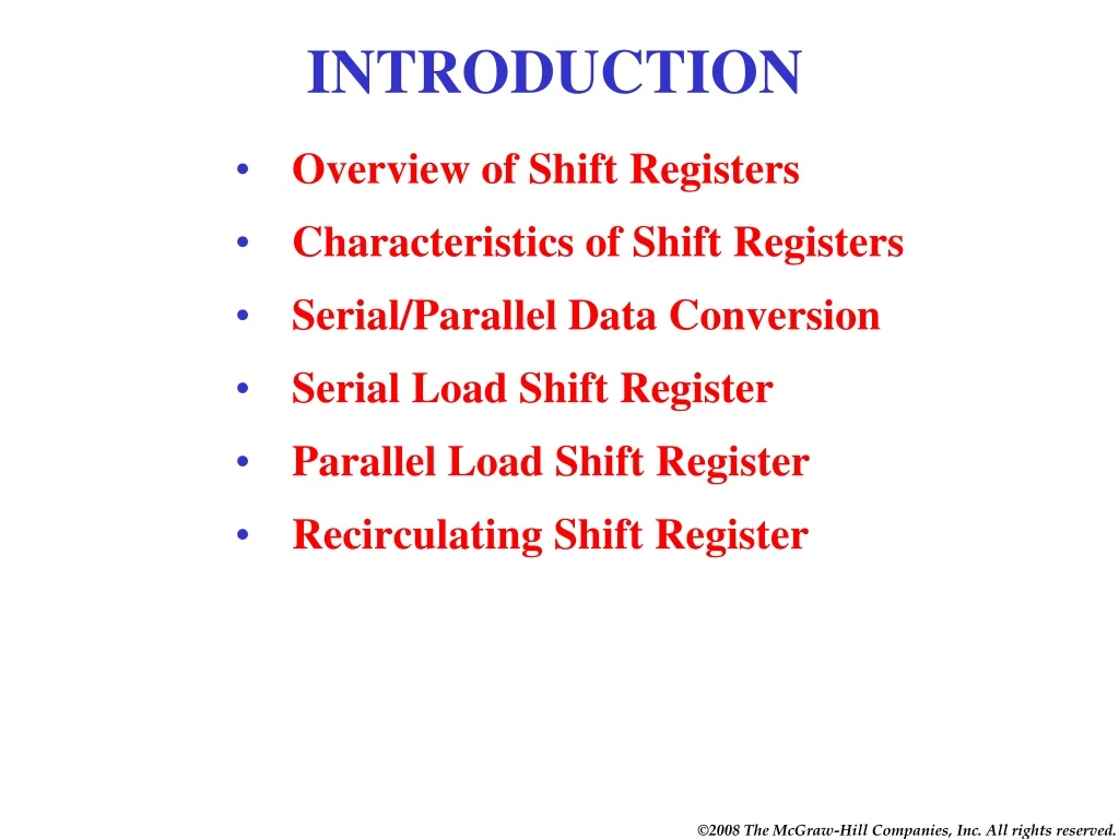
INTRODUCTION Overview of Shift Registers Characteristics of Shift Registers Serial/Parallel Data Conversion Serial Load Shift Register Parallel Load Shift Register Recirculating Shift Register
Overview of Shift Registers • A shift register is a sequential logic device made up of flip-flops that allows parallel or serial loading and serial or parallel outputs as well as shifting bit by bit. • Common tasks of shift registers: • Serial/Parallel Data Conversion • Parallel/Serial Data Conversion • As a memory device
Characteristics of Shift Registers • Number of bits (4-bit, 8-bit, etc.) • Loading • Serial • Parallel • Common modes of operation. • Parallel load • Shift right-serial load • Shift left-serial load
Parallel out Serial out Serial out Serial in 1 0 1 0 1 1 1 1 1 0 1 0 1 1 1 1 1 0 1 0 1 1 1 1 1 0 1 0 1 1 1 1 Parallel out Parallel in Parallel in Serial in Serial/Parallel Data Conversion Shift registers can be used to convert from serial-to-parallel or the reverse from parallel-to-serial.
QUIZ Q#1- This represents a ___ register. a. Parallel-in, parallel-out b. Serial-in, parallel-out Q#2- This represents a ___ register. a. Parallel-in, parallel-out b. Serial-in, serial-out Q#3- This represents a ___ register. a. Parallel-in, serial out b. Serial-in, parallel-out Q#4- This represents a ___ register. a. Parallel-in, serial out b. Parallel-in, parallel-out ANS: serial-in parallel-out ANS: serial-in serial-out ANS: parallel-in serial-out ANS: parallel-in parallel-out
Data = 0 Data = 0 Data = 1 Data = 1 Data = 0 Data = 1 Data = 0 Data = 1 Clock Pulse 5 Clock Pulse 8 Clock Pulse 7 Clock Pulse 1 Clock Pulse 3 Clock Pulse 6 Clock Pulse 4 Clock Pulse 2 Clear = 1 Clear = 1 Clear = 1 Clear = 1 Clear = 1 Clear = 0 Clear = 1 Clear = 1 Serial Load Shift Register Parallel outputs here. Order= A B C D 0 0 1 1 0 1 0 0 1 0 0 0 0 0 0 0 1 0 0 0 1 1 0 0 0 0 0 1 0 1 1 0 Inputs here: (1) Data (2) Clock (3) Clear 4-bit serial-in parallel out shift right shift register Clock input: Positive-edge triggering Clear input: Active = 0 Deactivated = 1 Note the use of D FFs. Clock (CLK) inputs wired in parallel. Clear (CLR) inputs can be activated with LOW or disabled with HIGH. Preset (PS) inputs deactivated.
Data = 0 Data = 1 Data = 1 Data = 0 Data = 1 Data = 1 Clock Pulse 5 Clock Pulse 4 Clock Pulse 1 Clock Pulse 3 Clock Pulse 2 Clock Pulse 6 Clear = 1 Clear = 0 Clear = 1 Clear = 1 Clear = 1 Clear = 1 QUIZ QUESTION #1 This is a ___ type shift register. A. Serial-in, parallel out B. Parallel-in, serial-out QUESTION #7 What is the 4-bit output (bit A on left, D on right) after pulse 6? QUESTION #2 What is the 4-bit output (bit A on left, D on right) after pulse 1? QUESTION #4 What is the 4-bit output (bit A on left, D on right) after pulse 3? QUESTION #3 What is the 4-bit output (bit A on left, D on right) after pulse 2? QUESTION #6 What is the 4-bit output (bit A on left, D on right) after pulse 5? QUESTION #5 What is the 4-bit output (bit A on left, D on right) after pulse 4? A: Serial-in, parallel-out A: 0100 A: 1000 A: 1100 A: 0000 A: 0010 A: 1001
Recirculating lines: Pass data from FFD to FFA on each clock pulse. Note the recirculating lines. Parallel Load Shift Register Outputs here. Order= A B C D Parallel data inputs (Active LOW) Clock input- H-to-L Clear input- Active LOW Note the use of J-K FFs. Clock (CLK) inputs wired in parallel. Clear (CLR) input activated with LOW. Parallel load inputs (A,B,C,D) are active LOW.
Parallel data inputs= all inactive Parallel data inputs= all inactive Parallel data inputs= all inactive Parallel data inputs= only B active Parallel data inputs= all inactive Parallel data inputs= C & D activated Parallel data inputs= all inactive Parallel data inputs= only D activated Clock pulse 8 Clock pulse 3 Clock pulse 7 Clock pulse 4 Clock pulse 1 Clock pulse 5 Clock pulse 6 Clock pulse 2 Clear input= 1 Clear input= 1 Clear input= 0 Clear input= 1 Clear input= 1 Clear input= 0 Clear input= 1 Clear input= 1 Recirculating Shift Register 0 0 1 1 0 0 0 0 1 1 0 0 0 1 1 0 1 0 0 1 0 0 1 1 0 0 0 0 0 1 0 0
Parallel data inputs= none active Parallel data inputs= none active Parallel data inputs= none active Parallel data inputs= none active Parallel data inputs= none active Parallel data inputs= B and C active Clock pulse 5 Clock pulse 4 Clock pulse 6 Clock pulse 3 Clock pulse 2 Clock pulse 1 Clear input= 1 Clear input= 0 Clear input= 1 Clear input= 1 Clear input= 1 Clear input= 1 QUIZ Q#1- After clock pulse 1, the output from the shift register will be ___. Q#2- After clock pulse 2, the output from the shift register will be ___. Q#3- After clock pulse 3, the output from the shift register will be ___. Q#4- After clock pulse 4, the output from the shift register will be ___. Q#5- After clock pulse 5, the output from the shift register will be ___. Q#6- After clock pulse 6, the output from the shift register will be ___. 0 1 1 0 1 1 0 0 1 0 0 1 0 0 1 1 0 1 1 0 0 0 0 0


