Download
1 / 36
410 likes | 643 Vues
Learn about classifying and organizing solids based on bonding types, crystal structures, lattice points, metallic and ionic structures, alloys, and intermetallic compounds. Explore molecular orbital approaches and the impact of ion size on ionic solid structures.

E N D
Lecture Presentation Chapter 12 Solids and Modern Materials James F. Kirby Quinnipiac University Hamden, CT
Classifying Solids Based on Bonds • Metallic solids are held together by a “sea” of collectively shared electrons. • Ionic solids are sets of cations and anions mutually attracted to one another. • Covalent-network solids are joined by an extensive network of covalent bonds. • Molecular solids are discrete molecules held together by weak forces.
Two Other Types of Solids • Polymers contain long chains of atoms connected by covalent bonds; the chains can be connected to other chains by weak forces. These molecules have different properties than small molecules or metallic or ionic compounds. • Nanomaterials are crystalline compounds with the crystals on the order of 1–100 nm; this gives them very different properties than larger crystalline materials.
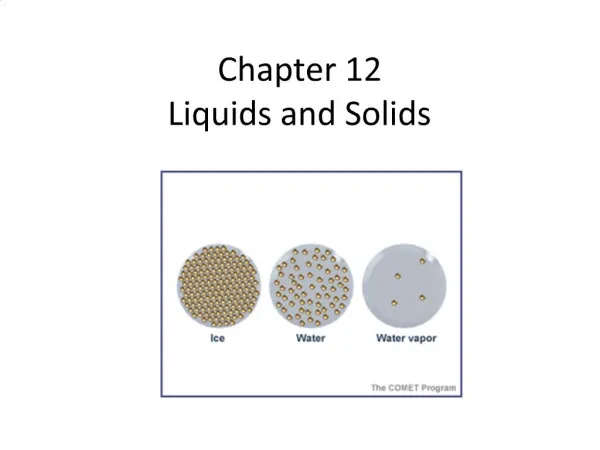
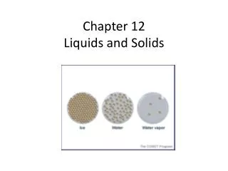
One Organization of Solids • Solids with a regular repeating pattern of atoms are crystalline. • Amorphous solids are characterized by a distinct lack of order in the arrangement of atoms. • Since crystalline solids have a regular pattern, they are of more interest to most chemists.
Unit Cell • The basis of a repeating pattern is the unit cell. • The structure of a crystalline solid is defined by • the size and shape of the unit cell. • the locations of atoms within the unit cell.
Lattice Points • Positions that define the overall structure of the crystalline compound are called lattice points. • Each lattice point has an identical environment. • Lattice vectors connect the points and define the unit cell. • The next slide shows how this works for five different two-dimensional lattices.
3-D Crystal Lattices • There are seven basic three-dimensional lattices: cubic, tetragonal, orthorhombic, rhombohedral, hexagonal, monoclinic, and triclinic.
Primitive vs. Centered Lattices • Primitive lattices have atoms only in the lattice points. • Centered lattices have atoms in another regular location, most commonly the body-center or the face-center.
Motifs Sometimes, the atoms are not on the lattice points, but the overall structure follows a particular unit cell. The groups of atoms that define the overall structure is called a motif.
Metallic Structure • The structures of many metals conform to one of the cubic unit cells: simple cubic, body-centered cubic, or face-centered cubic.
Cubic Structures • Not every part of an atom on a lattice point is completely within that unit cell. One can determine how many atoms are within each unit cell. • Eight cubes meet at a corner, therefore only 1/8 of that corner atom is within any one unit cell meeting there. • Two cubes meet at a face, therefore only 1/2 of that face atom is within any one unit cell meeting there. • A body-centered atom is entirely within the unit cell.
Close Packing • Nature does not like empty space! • The atoms in a crystal pack as close together as they can. • The two common types of packing seen are • cubic close-packed. • hexagonal close-packed.
Alloys • Alloys are materials that contain more than one element and have the characteristic properties of metals. • It is an important means employed to change the properties of certain metals.
Types of Alloys • Substitutional alloys: A second element takes the place of a metal atom. • Interstitial alloys: A second element fills a space in the lattice of metal atoms. • Heterogeneous alloys: components not dispersed uniformly
Intermetallic Compounds • compounds, not mixtures • distinct properties, definite composition (since they are compounds) • ordered, rather than randomly distributed
Metallic Bonding • One can think of a metal as a group of cations suspended in a sea of electrons. • The electrical and thermal conductivity, ductility, and malleability of metals is explained by this model.
A Molecular-Orbital Approach As the number of atoms in a chain increases, the energy gap between the bonding orbitals and between the antibonding orbitals disappears, resulting in a continuous band of energy. The approach seen here only takes into account s-orbital population.
MO Approach with More Orbitals • Most metals have d and p orbitals to consider. • Their MO diagrams lead to more bands that better explain conductivity and other properties of metals.
Ionic Solids • In ionic solids, the lattice comprises alternately charged ions. • Ionic solids have very high melting and boiling points and are quintessential crystals.
Ionic Solids • Most favorable structures have cation–anion distances as close as possible, but the anion–anion and cation–cation distances are maximized. • Three common structures for 1:1 salts: • CsCl structure • NaCl (rock salt) structure • zinc blende (ZnS) structure
Effect of Ion Size on Structure • The size of the cation compared to the anion (radius ratio) is the major factor in which structure is seen for ionic compounds.
Molecular Solids • Consist of atoms or molecules held together by weaker forces (dispersion, dipole–dipole, or hydrogen bonds). • Shape (ability to stack) matters for some physical properties, like boiling point. • Graphite is an example.
Covalent-Network Solids • Atoms are covalently bonded over large network distances with regular patterns of atoms. • Tend to have higher melting and boiling points. • Diamond is an example.
Semiconductors • They have a gap between the occupied MOs (valence band) and the unoccupied ones (conduction band). • Electrons must enter the conduction band for electron transfer. • Group IVA elements have gaps between the bands of 0.08 to 3.05 eV (7 to 300 kJ/mol). Note: Band gaps over 3.5 eV lead to the material being an insulator.
What Forms a Semiconductor? • Among elements, only Group IVA, all of which have 4 valence electrons, are semiconductors. • Inorganic semiconductors (like GaAs) tend to have an average of 4 valence electrons (3 for Ga, 5 for As).
Doping • changing the conductivity of semiconductors by adding an element with more or fewer electrons • n-type semiconductors have more electrons, so the negative charge travels in the conductance band. • p-type semiconductors have fewer electrons, so the “hole” travels in the valence band.
Polymers • Polymers are molecules of high molecular weight made by joining smaller molecules, called monomers. • There are two primary types of polymers: • Addition polymers are formed when a bond breaks, and the electrons in that bond make two new bonds. • Condensation polymers are formed when a small molecule is removed between two large molecules.
Bulk Properties of Polymers • The molecules are not straight lines—the longer the chain, the more twisting happens. • Chains can have a variety of lengths, and therefore a variety of molecular weights. • The material can be very flexible (plastics). • Short range order can lead to crystallinity in the solid.
Changing the Polymer’s Physical Properties • Chemically bonding chains of polymers to each other can stiffen and strengthen the substance. • In vulcanization, chains are cross-linked by short chains of sulfur atoms, making the rubber stronger.
Nanomaterials • Particles that have three dimensions on the 1–100 nm size • Their properties are the study of many labs around the world.
Semiconductors on the Nanoscale • Small molecules have discrete orbitals; macroscale materials have bands. Where does it switch over? • Theory tells us 1–10 nm (about 10–100 atoms). • Quantum dots are semiconductors this size.
Metals on the Nanoscale • Finely divided metals can have quite different properties than larger samples of metals. • Would you like “red gold” as in many old stained glass windows?
Carbon on the Nanoscale • Carbon nanotubes can be made with metallic or semiconducting properties without doping. • They are very strong materials. • Graphene has been discovered: single layers with the structure of graphite.