Download
1 / 1
10 likes | 266 Vues
MIAMI UNIVERSITY CENTER FOR NANOTECHNOLOGY. 3.5. 3. 2. 2.5. 1. 1.5. 0.9. 2. y (micron). 0.8. 1. 1.5. 0.7. c). p. 0.5. 0.6. a/2. 1. w. 0.5. Frequency (. 0.4. 0.5. 435nm. 435nm. 0.3. 440nm. 0.2. 0.5. 1. 1.5. 2. 2.5. 3. 3.5. 4. 4.5. x (micron). 0.1. 0. G.

E N D
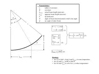
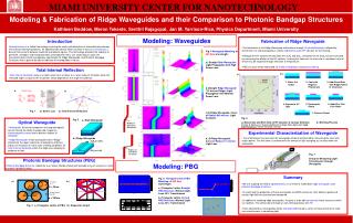
MIAMI UNIVERSITY CENTER FOR NANOTECHNOLOGY 3.5 3 2 2.5 1 1.5 0.9 2 y (micron) 0.8 1 1.5 0.7 c) p 0.5 0.6 a/2 1 w 0.5 Frequency ( 0.4 0.5 435nm 435nm 0.3 440nm 0.2 0.5 1 1.5 2 2.5 3 3.5 4 4.5 x (micron) 0.1 0 G X M G • Wafer Cut to Size 2. Coat with Negative Photoresist 3. Add Glass Slide with Ridge Pattern in Chromium 4. Expose to UV light 5. Develop the Resist 6. Add HF to Wet Etch Wafer a. b. 7. Remove Resist Fig. 6 a.) Selectivity and Etch Rate of HF solution at various Dilutions (Knotter, D. Martin et.al. "Selective Si3N4 etch in Single Wafer Application" Solid State Phenomena” Vol.103-104 (2005): 103-106.) b.) Etching Process Fig. 1 a.) Snell’s Law b.) Total Internal Reflection Fig. 2 a.) Slab Waveguide Si3N4 (n=2.02) b.) Ridge Waveguide SiO2 (n=1.46) 2.5 2 1.5 Air holes n=1 R 1.5 1 y (micron) 1 0.5 a 0.5 b Silicon Nitride n=2.02 0 0 0.5 1 1.5 2 2.5 3 3.5 4 4.5 5 x (micron) a 2 1.5 1 Amplitude 0.5 0 -3 -2 -1 0 1 2 3 s (micron) Modeling & Fabrication of Ridge Waveguides and their Comparison to Photonic Bandgap Structures Kathleen Beddow, Meron Tekeste, Senthil Rajagopal, Jan M. Yarrison-Rice, Physics Department, Miami University Modeling: Waveguides • Fabrication of Ridge Waveguide • The fabrication of the Ridge Waveguide will be done through UV photolithography followed by immersion of a slab waveguide in a dilute hydrofluoric acid (HF) solution for wet etching. • Although the HF solution will etch both the Si3N4 and SiO2, selectivity for the Si3N4 can be increased by increasing the dilution of the HF solution. In doing this however, the etch rate is sacrificed, some of which may be regained through elevation of temperature. • PBG structure will be fabricated via e-beam lithography and plasma etching. Introduction Optoelectronics is a field of technology involving the study and fabrication of microelectronic devices that interact with light (photons). An optoelectronic device either contains or acts as a transducer, a device that converts between electrical and optical signals. This technology provides the capacity to generate, transport, and manipulate data at exceptional rates. Our study focuses upon the characterization of both waveguides, specifically the Ridge Waveguide, and Photonic Bandgap Structures with a goal to be able to fabricate the waveguides in house. Fig. 4 Waveguide Modeling at 632.8nm wavelength: a.) Straight Slab Waveguide: Light Propagation with High Power Loss b.)Straight Ridge Waveguide (1.3 micron Ridge): Light Propagation with Minimal Power Loss c.)S-Ridge Waveguide, Curve of Radius 900 micron: Light Guidance d.) S-Ridge Waveguide, Curve of Radius 13 micron: Light Loss • Total Internal Reflection • Total Internal Reflection occurs as light travels from a higher to a lower index of refraction when the refracted angle is equal to 90o or greater, which depends on the angle of incidence. b.) a.) • Optical Waveguide • Waveguide: Structural component of integrated optical circuits having the ability to guide high frequency electromagnetic waves due to different indices of refraction. • Ridge Waveguide: A slab waveguide with a “Ridge” etched into the upper substrate, changing the effective indices of refraction on either side, creating conditions for Total Internal Reflection within the ridge area allowing for guidance of light. Radius of Curvature: 900 micron • Experimental Characterization of Waveguide • Once fabrication has occurred, the waveguide will be characterized by measuring the input and output power. This will allow us to determine the amount of light escaping as it travels down the waveguide. Radius of Curvature: 13 micron Fig. 7 Setup for Measuring Light Transmission through Waveguide • Photonic Bandgap Structures (PBG) • Photonic Bandgap Structure: Substrate (e.g. Silicon Nitride) etched with periodic array of air pores is used to create a photonic lattice. Modeling: PBG • Summary • We are studying the field of optoelectronics in an effort to model both ridgewaveguides and photonicbandgapstructures. • In examining the properties of these waveguides and PBG structures, their ability to guide and contain light will be examined and compared. • In addition to modeling ridge waveguides, the goal is to be able to fabricate these structures within our facilities. This will be done through an wet etching process with HF. • Once fabricated our waveguides will be characterized through a series of measurements to show their effectiveness in containing light. Fig. 5 Triangular Lattice PBG Modeling at 632.8nm wavelength: a.) Triangular Lattice Straight PBG Structure: Minimal Light Loss, 92% Transmission b.) Triangular Lattice Curved PBG Structure: Minimal Light Loss, 94% Transmission a.) b.) R = 75nm a = 257nm Fig. 3 a.) Triangular Lattice of PBG b.) Dispersion Graph