Impurity Segregation
Impurity Segregation. Where Co is the initial concentration of th impurity in the melt. Float Zone. www.mrsemicon.com/crystalgrowth.htm. www.tms.org/pubs/journals/JOM/9802/Li/. Impurity Segregation.

Impurity Segregation
E N D
Presentation Transcript
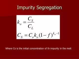
Impurity Segregation Where Co is the initial concentration of th impurity in the melt
Float Zone www.mrsemicon.com/crystalgrowth.htm www.tms.org/pubs/journals/JOM/9802/Li/
Impurity Segregation Where Co is the initial concentration of the impurity in the solid and L is the width of the melted region within RF coil
Bridgeman • Used for some compound semiconductors • Particularly those that have a high vapor pressure • Produced “D” shaped boules
Crystalline Defects • Point Defects • Vacancies • Impurities • Antisite Defects • Line Defects • Dislocations • Edge • Loop • Volume Defects • Voids • Screw Dislocations
Edge Dislocation http://courses.eas.ualberta.ca/eas421/lecturepages/mylonite.html
Screw Dislocation http://focus.aps.org/story/v20/st3
Strain induced Dislocations • The temperature profile across the diameter of a boule is not constant as the boule cools • the outer surface of the boule contracts at a different rate than the internal region • Thermal expansion differences produces edge dislocations within the boule • Typical pattern is a “W”
Strain due to Impurities • An impurity induces strain in the crystal because of differences in • ionic radius as compared to the atom it replaced • Compressive strain if the ionic radius is larger • Tensile strain if the ionic radius is smaller • local distortions because of Coulombic interactions • Both cause local modifications to Eg
Dislocation Count • When you purchase a wafer, one of the specifications is the EPD, Etch Pit Density • Dislocations etch more rapidly in acid than crystalline material • Values for EPD can run from essentially zero (FZ grown under microgravity conditions) to 106 cm-2 for some materials that are extremely difficult to grow. • Note that EPD of 106 cm-2 means that there is a dislocation approximately every 10mms.
Wafer Manufacturing • Boules are polished into cylinders • Aligned using an x-ray diffraction system • Cut into slices using a diamond edged saw • Slices are then polished smooth using a colloidal grit • Mechanical damage from sawing causes point defects that can coalesce into edge dislocations if not removed
http://www.tf.uni-kiel.de/matwis/amat/elmat_en/kap_6/backbone/r6_1_2.html#_dum_1http://www.tf.uni-kiel.de/matwis/amat/elmat_en/kap_6/backbone/r6_1_2.html#_dum_1
Epitaxial Material Growth • Liquid Phase Epitaxy (LPE) • Vapor Phase Epitaxy (VPE) • Molecular Beam Epitaxy (MBE) • Atomic Layer Deposition (ALD) or Atomic Layer Epitaxy (ALE) • Metal Organic Chemical Vapor Deposition (MOCVD) or Organometallic Vapor Phase Epitaxy (OMVPE)
MBE • Wafer is moved into the chamber using a magnetically coupled transfer rod • Evaporation and sublimation of source material under ultralow pressure conditions (10-10 torr) • Shutters in front of evaporation ovens allow vapor to enter chamber, temperature of oven determines vapor pressure • Condensation of material on to a heated wafer • Heat allows the atoms to move to appropriate sites to form a crystal
Schematic View http://web.tiscali.it/decartes/phd_html/III-Vms-mbe.png
http://ssel-front.eecs.umich.edu/Projects/proj00630002.jpg http://www.mse.engin.umich.edu/research/facilities/132/photo
Advantages • Slow growth rates • In-situ monitoring of growth • Extremely easy to prevent introduction of impurities
Disadvantages • Slow growth rates • Difficult to evaporate/sublimate some materials and hard to prevent the evaporation/sublimation of others • Hard to scale up for multiple wafers • Expensive
MOCVD • Growths are performed at room pressure or low pressure (10 mtorr-100 torr) • Wafers may rotate or be placed at a slant to the direction of gas flow • Inductive heating (RF coil) or conductive heating • Reactants are gases carried by N2 or H2 into chamber • If original source was a liquid, the carrier gas is bubbled through it to pick up vapor • Flow rates determines ratio of gas at wafer surface
Schematic of MOCVD System http://nsr.mij.mrs.org/1/24/figure1.gif
http://www.semiconductor-today.com/news_items/2008/FEB/VEECOe450.jpghttp://www.semiconductor-today.com/news_items/2008/FEB/VEECOe450.jpg
Advantages • Less expensive to operate • Growth rates are fast • Gas sources are inexpensive • Easy to scale up to multiple wafers
Disadvantages • Gas sources pose a potential health and safety hazard • A number are pyrophoric and AsH3 and PH3 are highly toxic • Difficult to grow hyperabrupt layers • Residual gases in chamber • Higher background impurity concentrations in grown layers
Misfit Dislocations • Occur when the difference between the lattice constant of the substrate and the epitaxial layers is larger than the critical thickness.
Carrier Mobility and Velocity • Mobility - the ease at which a carrier (electron or hole) moves in a semiconductor • Symbol: mn for electrons and mp for holes • Drift velocity – the speed at which a carrier moves in a crystal when an electric field is present • For electrons: vd = mn E • For holes: vd = mp E
L H W Va Va
Resistivity and Conductivity • Fundamental material properties
Resistivity n-type semiconductor p-type semiconductor
Diffusion • When there are changes in the concentration of electrons and/or holes along a piece of semiconductor • the Coulombic repulsion of the carriers force the carriers to flow towards the region with a lower concentration.
Mobility vs. Dopant Concentration in Silicon http://www.ioffe.ru/SVA/NSM/Semicond/Si/electric.html#Hall
Wafer Characterization • X-ray Diffraction • Crystal Orientation • Van der Pauw or Hall Measurements • Resistivity • Mobility • Four Point Probe • Resisitivity • Hot Point Probe • n or p-type material
Van der Pauw • Four equidistant Ohmic contacts • Contacts are small in area • Current is injected across the diagonal • Voltage is measured across the other diagonal Top view of Van der Pauw sample http://www.eeel.nist.gov/812/meas.htm#geom
Calculation • Resistance is determined with and without a magnetic field applied perpendicular to the sample. F is a correction factor that takes into account the geometric shape of the sample.
Hall Measurement • See http://www.eeel.nist.gov/812/hall.html for a more complete explanation http://www.sp.phy.cam.ac.uk/SPWeb/research/QHE.html
Calculation • Measurement of resistance is made while a magnetic field is applied perpendicular to the surface of the Hall sample. • The force applied causes a build-up of carriers along the sidewall of the sample • The magnitude of this buildup is also a function of the mobility of the carriers where A is the cross-sectional area.
Four Point Probe • Probe tips must make an Ohmic contact • Useful for Si • Not most compound semiconductors
Hot Point Probe • Simple method to determine whether material is n-type or p-type • Note that the sign of the Hall voltage, VH, and on D R13,24 in the Van der Pauw measurement also provide information on doping.